A serial bus can be more efficient than the traditional parallel bus. But there are challenges in representing and making sense of the serial data flow in the context of clock timing. These difficulties can be resolved by using the multi-channel capabilities of advanced oscilloscopes such as the Tektronix Series 3000 instruments.
The key to understanding and interpreting the serial data and clock streams lies in understanding the inner workings of each individual type of data bus. Specifically, consider the Serial Peripheral Interface (SPI) bus. It resembles the I2C bus, but there are significant differences. Both are organized around master/slave architectures. But the wiring between master and slaves is radically different.
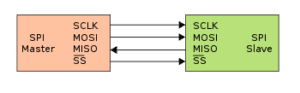
Typically, SPI operates with a single master device and a number of slaves, although as few as one slave is possible. The lines are as follows:
• A serial clock line runs from the master to each slave. The clock exists in the master and a square-wave clock signal is conveyed to the slave that is active. The clock frequency is chosen by the user, but it cannot be faster than permitted for the slowest slave device. So individual slave data sheets should be consulted in setting up the system.
• Master-out, slave-in (MOSI). This is the line that conveys data as transmitted by the master to whatever slave is active. The line runs to all slaves, but those that are not active ignore it.
• Master-in, slave-out (MISO). This line conveys data from the active slave to the master. Because MOSI and MISO are separate lines, data can be conveyed in both directions simultaneously, to the detriment of neither.
• Slave select (SS). A separate line is run to each slave. Normally, when the system powers up, a logic-high voltage from the master is present at the SS pin of each slave device. To activate a slave, the master switches the voltage on that SS line to logic low. This method of slave selection is in lieu of the addressing concept as implemented in the I2C bus.
The SPI bus is sometimes called a three-wire scheme, or a four-wire scheme if you count an SS line for a single slave. Needless to say, each of these wires is actually a two-wire circuit, so a ground return line is required, but it is not considered in the numerical nomenclature. A single grounded conductor will suffice to complete all of these circuits.
The Tektronix MDO Demo 1 Board provides numerous outputs including I2C and SPI bus clock and data signals. It is intended to go with the Tektronix MDO4000 Series oscilloscopes, but it also works well with the MDO3000 Series instruments.
The Tektronix MDO Demo 1 Board receives power via an unusual T-type USB cable that has dual USB type A connectors at one end. They insert into the two oscilloscope USB slots. The rationale is that the power requirements of the Demo Board 1 are such that if a standard USB cable were to be used, it would overload a single USB output at the oscilloscope.
One red and two green LEDs indicate reception of power from the oscilloscope and that the board is ready to go. There are numerous output terminals on the board. They are suitable for probe connection using probe hook tips and ground return lead alligator clips.

To display SPI bus signals, TPP 1000 10:1 probes plug into analog channel inputs One, Two and Three. All ground return leads connect to one of the board’s ground terminals, and the three probe tips are hooked onto the SPI clock, MISO and MOSI signal terminals. As always, the ground return leads should be connected first, before the probe tips.
One could use a fourth oscilloscope channel to display a slave-select signal. But because this signal is just a logic-high or logic-low voltage, it can be verified at both ends of the SPI bus using a standard high-impedance multimeter or logic probe.
The oscilloscope then displays the SPI data and clock signals. Using the Channel One, Channel Two and Channel Three scale buttons followed by Autoset, the pulses can be enlarged for readability, and the acquisition can be stopped to make the display more stable. The Wave Inspector knobs can be used to pan and zoom the traces for a closer look. Then it is a simple matter to compare points on the clock and data streams to ascertain the logic state (high or low) at any point in time. The vertical cursor, moved by turning Multipurpose Knob a, is helpful in seeing how these traces line up with respect to time.
We’ve seen how SPI serial bus data and clock signals can be visualized using an oscilloscope. The probes can be connected to similar terminals in a functioning (or non-functioning) piece of electronic equipment. (Be sure to turn the acquisition back to Run.)
Unlike I2C, there is no single standard for SPI. In the 1980s, it was developed by Motorola for use by the 68000 series microcontroller. SPI is a de facto rather than official standard, and as such it remains organic and subject to change.
Other manufacturers have introduced SPI with variations. So in implementing the design it is necessary to consult data sheets. For example, some slave devices require a falling edge in the SS signal to initiate communication. When there are multiple slave types, different initiating signals from the master are required. Like I2C, SPI is a short-haul serial bus. Because of its low power requirement, it is often used in cell phones, personal digital assistants and similar mobile equipment to implement interaction between CPU, display, keyboard and integrated circuits.
Variations include omitting the MISO line when communication from slave to master is unecessary. Also, the SS line is not needed when there is only a single slave, and the slave-select pin is grounded so it is always active.
While it is true that SPI is a synchronous serial interface (SSI), it differs radically from the SSI protocol, which is characterized by differential signaling and a single simplex communication channel.
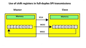 There is full-duplex transmission, both MOSI and MISO, during each clock signal. One bit is sent in each direction on the two separate lines. The usual procedure employs two shift registers, one in the master and one in the slave. Duplex transmission continues through a sufficient number of clock cycles to complete the transmission. In this manner, master and slave acquire the registers as conveyed over the two lines. If more data remains, the shift registers are reloaded and transmission commences anew.
This process continues through as many clock cycles as necessary, whereupon the master allows the select signal to go to logic high, deselecting the slave. Transmissions are often 8-bit, but there are variations such as 12-bit for many DACs and ADCs, and 16-bit for touchscreen controllers.
Because of hardware and de facto protocol differences, the SPI bus has a spectrum of advantages and disadvantages with respect to I2C and other bus types. Advantages include full-duplex capability merely by adding another line. Moreover, there is good signal integrity, high speed transmission, and more potential data transmission compared to I2C. Also, message content is unlimited and not restricted to 8-bit data units. Generally, the power requirement is less than in I2C because pull-up resistors are unnecessary. SPI is also dependable because it needs no arbitration, and there is no need for unique slave addresses. Because there is no maximum clock speed aside from slave device constraints, there is the potential for high-speed operation.
As in any technology, there are disadvantages with respect to some other protocols. Because there is no slave acknowledgement, in the event of slave or cabling failure, the master, unaware that something is wrong, could be talking into a void with no listener. Also, the lack of a single formalized standard can make conformance validation impractical. Also, the existance of numerous unregulated SI variations can make the acquisition of hardware problematic.
Down the road, it is conceivable SPI could see a greater degree of codification. This development will mean further SPI enhancements that could reduce the confusion that now exists. That said, as currently implemented, SPI is quite user-friendly, particularly in its requirement for little power.

when to use what combination of phase and polarity of clock for data transfer,how to decide?
The slave data sheet will specify phasing and polarity of the clock. Some devices need the clock pulses to idle high and signify a clock pulse by going on a low-to-high transistion, others are the opposite, a few will auto-sense the clock polarity and timing based on when CE (Chip Enable) is enabled. Or sometimes it’s CE/NOT (low to enable). You just gotta’ read the data sheet of the slave device and program the master protocol accordingly or add inverting logic if needed.