• Skip to primary navigation
  • Skip to main content
  • Skip to primary sidebar
  • Skip to footer
  • Advertise
  • Subscribe

Test & Measurement Tips

Oscilloscopes, electronics engineering industry news, how-to EE articles and electronics resources

  • Oscilloscopes
    • Analog Oscilloscope
    • Digital Oscilloscope
    • Handheld Oscilloscope
    • Mixed-signal Oscilloscope
    • PC-based Oscilloscopes – PCO
  • Design
  • Calibration
  • Meters & Testers
  • Test Equipment
  • Learn
    • eBooks/Tech Tips
    • FAQs
    • EE Training Days
    • Learning Center
    • Tech Toolboxes
    • Webinars & Digital Events
  • Video
    • EE Videos
    • Teardown Videos
  • Resources
    • Design Guide Library
    • Digital Issues
    • Engineering Diversity & Inclusion
    • Leap Awards
    • White Papers
  • Subscribe
You are here: Home / Featured / Basics of CMOS

Basics of CMOS

October 31, 2014 By David Herres 1 Comment

By David Herres

Complementary metal-oxide semiconductor (CMOS) is a highly successful strategy for combining complementary and symmetrical pairs of p-type and n-type MOSFETs to create logic functions. A CMOS transistor pair is typically a building block for integrated circuits. Among its many applications are image sensors in digital cameras, data converters and transceivers.

A static CMOS inverter.

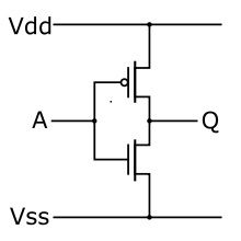
In a common form, one p-type MOSFET and one n-type MOSFET are wired together to make a complementary and symmetrical pair. The defining quality of a p-type MOSFET is that there is low resistance between the source and drain when a low voltage is applied at the gate. Conversely, in an n-Type MOSFET, there is high resistance between source and drain when the gate voltage is low, and low resistance between the source and drain when the gate voltage is high.

By connecting both gates together and both drains together, as shown in the schematic, the two opposite types of MOSFET’s work in concert. When high voltage is applied to the gates, the  n-type MOSFET will conduct and the P-type MOSFET will not conduct. A low voltage on the gates will cause the opposite, i.e. the n-type MOSFET will not conduct and the p-type will.

cmos cross sectgdi
A cross section of two transistors in an n-well CMOS gate. The body connection is typically tied to the source in discrete devices but not necessarily in CMOS integrated circuits.

A CMOS gate is composed of two opposite type MOSFETs. CMOS technology can also be found in analog uses such as op amps and mixed-signal analog/digital circuits.

The upshot of all this is that one of the two MOSFETs is always off. And because they are in series with respect to the power supply, the combination consumes little power. (The interesting thing about a CMOS pair is that they are in series with respect to the power supply and in parallel with respect to the signal.) The two devices in series do not conduct, except briefly during transitions. At these moments, there is a short high-intensity spike. It may create a problem if  not accounted for and mitigated. RF interference may adversely affect nearby electronic equipment and there can be power quality issues.

Despite all this, CMOS technology has been exactly the right solution at the right time. Its average power consumption, heat dissipation and temperature rise are comparatively low, permitting massive integration of devices on a single small crystalline silicon substrate. This achievement fit the bill to satisfy ongoing needs for increased bandwidth and high-speed connectivity.

You may also like:

  • measuring CMOS power dissipation
    Measuring CMOS power use
  • CCDs and microbolometers
    The difference between CCD and microbolometer thermal imaging
  • cmos noise margin
    Basics of CMOS and measuring CMOS logic parameters
  • ccd cmos image sensors
    How to measure CCD and CMOS image sensor qualities
  • ccd imager chip
    The difference between CCD and CMOS image sensing

Filed Under: FAQ, Featured, New Articles

Reader Interactions

Leave a Reply Cancel reply

You must be logged in to post a comment.

Primary Sidebar

Featured Contributions

Why engineers need IC ESD and TLP data

Verify, test, and troubleshoot 5G Wi-Fi FWA gateways

How to build and manage a top-notch test team

How to use remote sensing for DC programmable power supplies

The factors of accurate measurements

More Featured Contributions

EE TECH TOOLBOX

“ee
Tech Toolbox: Power Efficiency
Discover proven strategies for power conversion, wide bandgap devices, and motor control — balancing performance, cost, and sustainability across industrial, automotive, and IoT systems.

EE TRAINING CENTER

EE Learning Center
“test
EXPAND YOUR KNOWLEDGE AND STAY CONNECTED
Get the latest info on technologies, tools and strategies for EE professionals.
bills blog

RSS Current Electro-Tech-Online.com Discussions

  • ESP32-S3 started outputting NMEA GPS location frames after EMC disturbance — what mode is this?
  • TraxMaker Pro? I only have the non-Pro version. Looking for the Pro version that has the integrated pick and place coordinates export.
  • Can a small solar panel safely trickle-charge old NiMH AA batteries?
  • desoldering
  • Need a fresh eye on my first PCB

Footer

EE World Online Network

  • 5G Technology World
  • EE World Online
  • Engineers Garage
  • Analog IC Tips
  • Battery Power Tips
  • Connector Tips
  • EDA Board Forums
  • Electro Tech Online Forums
  • EV Engineering
  • Microcontroller Tips
  • Power Electronic Tips
  • Sensor Tips

Test & Measurement Tips

  • Subscribe to our newsletter
  • Advertise with us
  • Contact us
  • About us

Copyright © 2025 · WTWH Media LLC and its licensors. All rights reserved.
The material on this site may not be reproduced, distributed, transmitted, cached or otherwise used, except with the prior written permission of WTWH Media.

Privacy Policy