By David Herres
The FET, discussed in a previous article, was widely used for a few short years, from its introduction in 1947 until it was abruptly eclipsed upon the introduction of the metal-oxide semiconducting field-effect transistor (MOSFET) in 1960. The MOSFET is like the FET, only more so. Structurally and functionally, they are similar. The defining difference is that the MOSFET has even higher, almost astronomical, input impedance. This value can be as high as 100 Ω, greater than the insulation covering a high-voltage underground transmission line. Relatively speaking, only a very few electrons are let through per second. This is because of the high ohmic value of the insulation between gate and channel, the small size of the device and the low working voltage.


In the P-channel MOSFET schematic, the arrow points outward. In the N-channel device schematic, the arrow points inward.
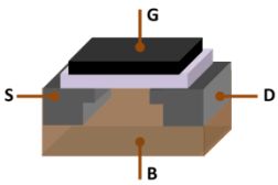
The MOSFET’s high input impedance comes from the fact that the gate is insulated from the rest of the device by a thin layer of silicon dioxide. At one time the insulating material was a metal oxide. Despite the change, the original terminology persists.
The electrical parameters have changed but the basic principles are the same. Channel current is governed by voltage on the gate, as referenced to the source. In placing an electrostatic charge on such a small body, the current flow is almost nonexistent. Because of its high impedance, the MOSFET places almost no load on the upstream device. Moreover, the MOSFET has a low output impedance. Consequently, it is a stiff source that will not be loaded by a downstream device.
The MOSFET can operate in either a depletion or enhancement mode. (The enhancement mode is much more common.) When there is no voltage between gate and source, the enhancement-mode MOSFET does not conduct. Conversely, when this voltage exceeds the threshold level, the channel becomes conductive.
When the channel contains electrons functioning as current carriers it is called an nMOSFET or nMOS device. When it contains holes it is called a pMOSFET or pMOS device. The current carriers are opposite in type to the substrate, so nMOS has a p-type substrate, and pMOS has an n-type substrate.
In a depletion-mode MOSFET, the current flow ceases altogether when the voltage reaches pinch-off. The channel consists of carriers in a surface impurity layer opposing that of the substrate. Conductivity drops on application of a field that depletes carriers from this surface layer.
Actually the MOSFET is typically seen not as a discrete device, but sits within the vast interior architecture of integrated circuits (ICs), where it may number in the billions. As we shall see in a future article, the MOSFET is generally used in the complementary metal oxide semiconductor (CMOS) configuration. CMOS currently involves much less power loss and resulting temperature rise, permitting greater amounts of integration than at one time were dreamed possible.

Leave a Reply
You must be logged in to post a comment.