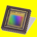
Complementary metal-oxide semiconductor (CMOS) fabrication uses p-type and n-type complementary and symmetrical pairs to implement logic functions. The fundamental building block of the CMOS circuit is the MOSFET semiconductor, which enables it to operate at far lower current levels than bipolar transistors. This current reduction comes via pairs of p-type and n-type MOSFETs connected gate-to-gate and drain-to-drain. The two opposing types of MOSFETs work together when the two gates and the two drains are shorted together.
 In a p-type MOSFET, when a low voltage is applied to the gate, resistance between source and drain is low. In contrast, in an n-type MOSFET, a high gate voltage causes low resistance between source and drain. When high voltage is applied to the gates, the n-type MOSFET conducts and the p-type MOSFET doesn’t. When low voltage is applied, only the p-type MOSFET conducts.
Accordingly, one of the MOSFETs is always off. Because they are in series with respect to power and in parallel with respect to signal, the signal is always on and the power is always off except during brief transitions. Most of the time, this configuration conducts little current and dissipates littler power. So vast numbers of MOSFETs can be squeezed onto ICs without large heat sinks or active cooling.
A downside, easily mitigated, is that during the brief transitions, relatively high-voltage spikes occur, and at today’s high frequencies, they are abundant, potentially affecting nearby receivers and creating power-quality anomalies. To avoid such difficulties, the usual practice is to add bypass capacitors to the signal lines.
 CMOS IC chips have a high immunity to noise. The reason is the voltage transfer curve for a typical CMOS logic gate. It is characterized by a transition region that is almost vertical. This steep transition is what imparts the high noise immunity. The threshold voltage depends on the supply voltage and is approximately half the supply voltage.
The typical quiescent (static) power dissipation (power dissipation of a device that is not changing logic states) of CMOS ICs operating at 5 V are on the order of 50 nW at room temperature. However, as the frequency of switching increases, dynamic power dissipation becomes important. The input impedance, in either state, of CMOS gates is typically on the order of 1012 Ω. The input capacitance is on the order of 10 pF. The output impedance depends on the particular device and is on the order of 5 kΩ for either state.
CMOS devices have relatively long propagation delays to their high output impedance. Typical delay times are in the 60 nsec range for VDD = 5 V and around 25 nsec for VDD = 10 V. Doubling the supply voltage more than doubles the speed of a CMOS gate. The rise and fall transition times typically range from 75 to 150 nsec for VDD = 5 V.
A point to note is that CMOS logic has floating inputs. If left unconnected, they can increase susceptibility to noise and lead to excessive power dissipation. So chip data sheets generally advise connecting all unused inputs to VDD or VSS, as appropriate.
CMOS devices generally have a fan-out exceeding 50 because of their low input current requirement. However, there is some power dissipated in charging and discharging the capacitance of CMOS inputs during logic transitions. So the greater the fan-out the longer the propagation delay.
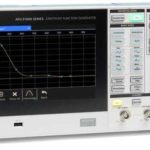
 It is easy to verify the basic operating parameters of CMOS logic chips using just an oscilloscope and a function generator. For example, we can display the characteristic curve of a CMOS inverter by setting a generator to produce a sawtooth waveform. For a simple inverter IC such as the CD4069UB, the amplitude should be adjusted to produce positive voltages in the range 0 V to 5 V.
Connect the inverter output Vout to the Channel 2 input and Vin to the Channel 1 input of the scope. You want to plot Channel 1 vs. Channel 2, so the scope must be in XY mode. The resulting plot of Vout vs. Vin is the gate voltage transfer curve.
Different sections of the characteristic curve correspond to different operating modes for the two MOSFETs making up the CMOS gate.
 Another simple circuit can be used to figure the CMOS gate noise margin. Consider a CD4001B CMOS Quad two-Input NOR Gate. One method is to set a square wave signal at minimum amplitude and put it at the input of a CMOS logic gate (or a series of them for an easier measurement). The square wave goes to one scope channel, the output of the last CMOS gate to the other channel. Then you slowly increase the square wave amplitude. When a pulse first appears on the output, the amplitude of the input pulse at that point is the noise margin.
 A simpler test setup reveals CMOS gate propagation delay. The higher the frequency, the longer the propagation delay, so it might be best to use a higher-frequency square wave (hundreds of kilohertz or higher) to more easily see the effect. Another way to get a more pronounced read out is to send the square wave through a string of CMOS gates, then divide the delay reading by the number of gates in the string to get an average propagation delay per gate.
At any rate, the test setup puts the input to the gates on one scope channel, the output of the last gate in the string on the other. With both channels displayed on the screen, adjust the scope to give a close-up of the output waveforms at the first and last gates during both transitions from HIGH to LOW and LOW to HIGH. The amount of delay between corresponding transition points, divided by the number of gates you put in the string, is the average propagation delay per gate.


Leave a Reply
You must be logged in to post a comment.