Voltage can be doubled (and therefore multiplied by any power of two using cascading devices) through purely electronic means without resorting to a transformer. Voltage-current ratios apply, so doubling is not a question of getting free electrical energy that did not previously exist. Doubling the voltage and thus reducing the current available at the output is sometimes not a good thing, but often this is not an issue.

There are many doubler circuit variations, but all voltage doublers and multipliers have similar operating principles.
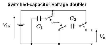
The switched-capacitor voltage doubler runs from a dc input. Two capacitors charge to the input voltage while in parallel. Then, when the two switches are thrown simultaneously, they are isolated from the input, connected to the output and placed in series so in discharging, twice the input appears at the output. Obviously, lacking a demon to throw the switches at a rapid rate, manually-operated switches are not practical. A variety of real-world switching strategies have been implemented:
In ac-to-dc converters, alternating current at the input, besides supplying the voltage to be doubled, also accomplishes switching by means of oscillating polarities.
An internal chopper circuit can convert dc to ac before application to the voltage doubler section.
An external clock (often also performing other functions on the same circuit board) can achieve chopping and voltage multiplication.
In integrated circuits, MOSFETs frequently provide the switching action.

A voltage tripler can be built by stacking a voltage doubler, typically 5-Vpp at 1 kHz, and a simple half-wave rectifier, composed of a diode and capacitor connected from one input terminal to the opposite output terminal. The 10-V doubler output in series with the 5-V rectifier output provides 15 V at the tripler output. Doublers and triplers, cascaded, provide theoretically an infinite number of integer outputs.

In prototyping line-driven power supplies even with no transformer, there is a potential shock hazard. Beware also that electrolytic capacitors will explode if polarity is reversed. Cascaded multiplier circuits should be built in a ladder configuration so the progressively increasing voltage potential cannot arc across individual lower-potential sections. That way, the entire ladder is not destroyed by a single shorted diode or capacitor. Without the ladder configuration, a single short could burn out successive adjacent components, eventually applying over-voltage to the entire multiplier, test equipment and experimenter.
Voltage multipliers can generate millions of volts for high-energy experiments. Transformer technology in such applications would require elaborate liquid-filled enclosures and high-voltage insulation.
 The most widely-used method for generating high-voltage, low-current output is the multistage Cockcroft-Walton multiplier due to its low cost and modest insulation requirements. The voltage drops abruptly when fed into a low-impedance load. It was used extensively in CRT TV sets where a 30-kV second anode accelerating voltage was required notwithstanding the high ripple. Because stepped voltages are available, this source has been used in particle accelerators and for biasing in photomultiplier tubes. They are used to power such diverse equipment as particle accelerators, X-ray machines, cathode-ray tube TVs, magnetrons in microwave ovens, photocopiers, and bug zappers.
 Multi-stage Cockcroft-Walton voltage multipliers can be configured in a single ladder. This voltage multiplier uses a low-voltage pulsating dc at the input to produce theoretically unlimited output voltage. With each change in polarity, current flows through successive diodes to charge additional capacitors, all the way to the end. After initial energization, a definite amount of time is required to charge the entire assembly. Each capacitor has a time constant and the total time depends upon applied voltage, capacitance of the capacitors and length of the ladder. Intermediate taps can be installed to access intermediate voltages.
The Cockcroft-Walton voltage multiplier is one type among many charge pumps, named for the characteristic manner in which they force an electrical charge along a pipe-like series of capacitors, each of which stores the charge until the polarity reverses, whereupon they discharge.
In general, a charge pump is a voltage multiplier that is optimized for use with a dc input. You could chop the dc by means of an oscillator and apply it to a transformer, but one of the advantages in voltage multiplication technology is that the heavy transformer with it massive space requirements is eliminated. In our age of mobile devices, the charge pump is an asset.
A charge pump can be based on diodes, but the usual configuration involves switched MOSFETs with small ceramic capacitors. Charge pump efficiency is high, as required in cell phones. In designs using discrete components, Schottky diodes, formed by the junction of a semiconductor with metal, are preferred because of their low forward voltage drop. In a charge pump implemented as an IC, high-efficiency MOSFETs with low input impedance are common-place.
A charge pump can also invert polarity at the output with respect to the input. Besides boosting voltage, a charge pump can halve or, in cascade configuration, divide input by any whole integer. Use of high clock frequencies permits use of lower capacitance because of the shorter time constants. Output voltage is regulated by changes in the clock output duty cycle. One advantage of the charge pump is that it can shift between buck and boost modes, compensating for battery drain between charges.
Where multiple dc voltage outputs are needed, the charge pump is far more compact and less expensive than a linear power supply, which is encumbered by a transformer with secondary taps. Capacitors can be electrolytic or ceramic depending upon the switching speed.
Voltage doublers and inverters can be built around the 555 timer IC with two external diodes and three or four external capacitors. When positive and negative supplies are required to power an op-amp, the charge pump can be configured as a voltage inverter.
If an IC requires multiple voltages as for example a single high-current primary source and auxiliary low-current sources, a charge pump is the ideal power converter. Other applications are EEPROMs and flash memories.
With fewer components and no inductor, the simple charge pump requires less PCB space and it is more efficient than the linear power supply.
The downsides are modest: It is limited to fractional-amp loads and like all SMPSs, it generates some electromagnetic interference and is not as efficient as similar power supplies built around inductors, which can power larger loads but are more expensive.
All voltage multipliers use a configuration comprised of diodes and capacitors to multiply to a voltage level desired by the end-user, a peak ac voltage (derived from, in order of increasing variability, utility, onsite backup or local inverter) or battery-supplied, hydro or wild dc from a wind turbine.
Diodes and capacitors are used in concert to form voltage multipliers. These circuits are capable of multiplying the voltage by a factor of four or more to produce theoretically any voltage, well into the kilovolt range. The technology is used to good effect in high-voltage transcontinental electrical distribution to make voltage and system transitions. But the diodes and capacitors must have adequate reverse-breakdown ratings of twice peak voltage because of the high voltages produced in multi-stage equipment.
In designing and diagnosing voltage multipliers, mixed-signal oscilloscopes or related instrumentation are essential in visualizing digital in juxtaposition with analog signals. For example, on a small scale, intermittent power-supply operation can disrupt digital data flow, and by displaying both waveforms in real time, these problems can be analyzed.


Leave a Reply
You must be logged in to post a comment.