Transistor-transistor logic (TTL) and complementary metal oxide semiconductor (CMOS) logic are the principal types of integrated circuit-based logic gates implemented in digital circuitry. TTL employs bipolar junction transistor technology while CMOS uses the field-effect transistor concept at the input. TTL consumes far more power than CMOS, which is one reason CMOS has eclipsed TTL as the dominant technology. Still, there is a lot of TTL around, so both must be considered.
Each logic family is characterized by several important parameters. Fan-in is the maximum number of inputs a gate can handle. Physical considerations limit fan-in, but practicalities such as the number of pins on IC packages generally are more important. TTL NAND gates typically provide 1, 2, 4, or 8 inputs.
Fan-out specifies how many standard loads the output of a gate can drive without a problem. A standard load is defined as the amount of current necessary to drive an input of another gate in the same logic family. The nature of TTL gates dictates the use of two different fanout values, one for HIGH outputs and one for LOW outputs. Typically at most 40 µA flows into an input at logic 1 and the driving output must provide this current. For logic 0, at most 1.6 mA flows from the input which the driving output must sink or accept.
By convention, the current flowing into an input or output is considered positive while a current flowing out of an input or output is considered negative. A typical TTL gate can source 400 µA of current and can sink 16 mA. Exceeding these fan-out limits may cause incorrect voltage levels at the output. The lower value of the two fanout values determines the fanout of the gate.
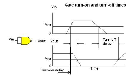 The propagation delay time for a gate specifies how long it takes the output to respond to a change in an input. In all practical gates, there’s a time lag between an input change and the corresponding output response. The time span between when the input and output
change states isn’t a satisfactory measure of the delay time for two reasons.
First, the input signals to gates and the output signals produced by gates don’t resemble the idealized pulses studied in theory. The transitions between HIGH and LOW voltage levels have nonzero rise and fall times. The time needed for a signal to rise from 10% to 90% of its final value is called the rise time. The fall time is the period required for the signal to fall from 90% to 10% of its initial value.
Second, the input voltage to a gate need only reach the threshold voltage level before the device begins to change state. Consequently, the delay time is measured with respect to a
reference voltage level called the threshold voltage.
A phenomenon associated with TTL devices is current spiking. When the output of a TTL
device is HIGH, the IC draws a constant supply current, 4 mA for a 7400 NAND gate. When the output is LOW, the device draws a different constant supply current, 12 mA for the 7400 IC. However, the chip draws an additional burst of current during the transition when the gate output changes state. The result is current spikes (narrow pulses) in the power supply line. The largest spike happens in the LOW-to-HIGH transition.
The usual practice to prevent these current spikes from appearing as noise is to add one decoupling capacitor (0.01 to 0.1 µF) from power to ground near the IC pins for each five to ten IC packages.
Any loads on the outputs of gates degrade the output signal. There is capacitive loading if the load on the output of a gate has a capacitive component. This external load capacitance component can be from other logic devices, stray wiring capacitance, or similar factors. The effect of capacitive loads is to lengthen the rise and fall times of signals,
thereby lengthening propagation delay times and slowing operation speed.
Resistive loading is present when the load impedance contains a resistive component, such as that associated with other logic devices. Resistive loading reduces noise margins and output voltages.
Performance factors vary depending on the logic family. For example, the input impedance, in either state, of CMOS gates is typically 1012 Ω. The input capacitance
is 5 pF. The output impedance depends on the particular device, and is on the order of 1 kΩ, for either state.
In contrast, for TTL, there is no input impedance defined. The input is usually just modeled as a capacitor.
The propagation delay times for CMOS devices are significant because of their high output
impedance. Typical delay times are 60 nsec for 5-V logic, 25 nsec operating at 10 V. Doubling the supply voltage more than doubles the speed of a CMOS gate.
The fan-out of CMOS devices is usually greater than 50 because CMOS input current requirements are on the order of picoamps. However, it takes current to charge and discharge the capacitance of CMOS inputs during logic transitions. So, the greater the fan-out the more propagation delay. One rule of thumb assumes the load will be 5 pF per CMOS input plus 5 to 15 pF for stray wiring capacitance.
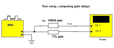 It’s possible to evaluate several of these parameters with a simple oscilloscope. To see rise and fall times, try applying, say, a 300 kHz square wave from a function generator to the inputs of a CMOS gate and to the inputs of a TTL gate. (This frequency should be low enough for even low-end AWGs and scopes.) Use the oscilloscope to display the outputs from both gates simultaneously. You should be able to see a significant difference in the rise and fall of the outputs from the two chips.
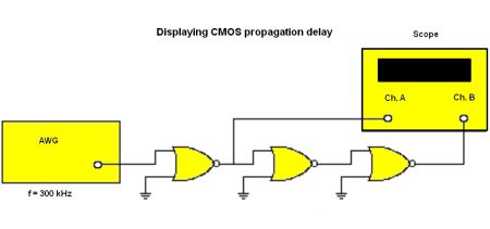 Similarly, you should be able to see the propagation delay through two CMOS gates by feeding the signal of one to the input of the other. Use the AFG to generate a clock pulse for an input. With the oscilloscope in the voltage vs. time format, you can display detailed close-ups of the output waveforms at the first and last gates, during both transitions from HIGH to LOW and LOW to HIGH.
To see capacitive loading, connect the AWG producing pulses to two TTL NAND gates and a 300 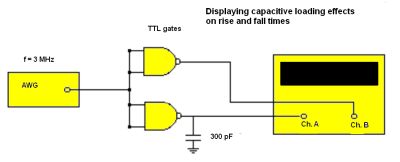 pF capacitor to the output of one of the NAND gates. The capacitor will simulate the capacitive loading component induced by several gate inputs. You can display the two outputs simultaneously to see the effect of capacitive loading on rise and fall times.
To see the current spiking that can happen in TTL gates, power up a TTL chip and make sure nothing is connected to its input or its output. Set the pulse generator in the AWG to
300 kHz and connect it to all the inputs of all four gates on the TTL IC. Use the scope to simultaneously observe the power supply voltage at the VSS pin on the TTL chip and the output of one of its NAND gates.

This is a good tutorial article, a good starting point for those interested in applying readily available test instruments such as AWGs and DSOs for measurements on digital logic. It stays away from naming favorites for different instruments (specific suppliers and model numbers) but provides useful “how-to” advice for basic measurements.