Today, about 95% of all digital cameras use CMOS image sensors with the rest employing CCDs. From the standpoint of sensor outputs, the main difference between CMOS and CCD sensors is that each pixel in a CMOS sensor has its own readout circuit next to the photosensitive area. In CCDs, charge collected in individual pixels is subsequently shifted along transfer channels under the influence of voltages applied to a gate structure for readout.
To understand image sensor measurements you must grasp the basic structure of these sensor technologies. Also, a point to note is that there are only limited opportunities for making measurements of image sensors built into end-use equipment such as mobile phones. That’s because there’s no direct access to sensor outputs. Measurements typically take place on the sensor chips themselves. So we’ll quickly review a few fundamentals of these ICs.
 CCD chips contain a large number of light-sensing (pixel) elements arranged in a two-dimensional array. The elements trap and hold photon-induced charge carriers when biased correctly. The fundamental light-sensing unit of the CCD is a metal oxide semiconductor (MOS) capacitor operated as a photodiode and charge-carrier storage device. Reverse bias causes negatively charged electrons to migrate to an area underneath a positively charged gate electrode. Electrons liberated by photon interaction get stored in the depletion region up to what’s called the full-well reservoir capacity.
In a complete CCD, individual sensing elements in the array are segregated in one dimension by voltages applied to the surface electrodes. They are also electrically isolated from their neighbors in the other direction by insulating barriers, or channel stops, within the silicon substrate.
Light-sensing photodiode elements of the CCD respond to incident photons by absorbing much of their energy, thereby liberating electrons. The process forms electron-deficient sites (holes) within the silicon crystal lattice, one electron-hole pair from each absorbed photon. The resulting charge that accumulates in each pixel is linearly proportional to the number of incident photons.
External voltages applied to each pixel’s electrodes control the storage and movement of accumulated charges. Although either negatively charged electrons or positively charged holes can be accumulated (depending on the CCD design), the charges generated by incident light are usually referred to as photoelectrons.
The image generation process of a CCD is often divided into four stages: charge generation through photon interaction with the device photosensors, collection and storage of the liberated charge, charge transfer, and charge measurement. First, electrons and holes are generated in response to incident photons in the depletion region of the MOS capacitor, and liberated electrons migrate into a potential well formed beneath an adjacent positively-biased gate electrode. There is system of aluminum or (transparent) polysilicon surface-gate electrodes that are separated from the charge carrying channels buried within a layer of insulating silicon dioxide placed between the gate structure and the silicon substrate.
Electrons generated in the depletion region are initially collected into electrically positive potential wells associated with each pixel. During readout, the collected charge is subsequently shifted along the transfer channels as voltages are applied to the gate structure with the proper timing.
Stored charge from each sense element in a CCD are transferred to a readout node via a charge-transfer process. Charge is moved across the device by manipulating voltages on the capacitor gates in a pattern that causes charge to spill from one capacitor to the next, or from one row of capacitors to the next. Because the CCD is a serial device, the charge packets are read out one at a time.
A combination of parallel and serial transfers deliver each sensor element’s charge packet, in sequence, to a single measuring node. The CCD electrode (gate) network forms a shift register for charge transfer. The charge-coupled shift of the entire parallel register moves the row of pixel charges nearest the register edge into a specialized single row of pixels along one edge of the chip called the serial register. From this row charge packets move in sequence to an on-chip amplifier for measurement. Once emptied, the serial register is refilled by another row-shift of the parallel register, and the cycle repeats.
The need for nearly perfect charge transfer complicates the manufacture of CCD image sensors.
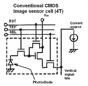
CMOS imagers avoid the problem. The simplest CMOS imagers employed pixels without amplification, with each pixel consisting of a photodiode and a MOSFET switch. Today’s CMOS sensors are called active pixel sensors (APS), with each pixel containing one or more MOSFET amps which convert the photo-generated charge to a voltage, amplify the signal voltage, and reduce noise. CMOS sensors also use a special kind of photodetector called a pinned photodiode that is optimized for low lag, low noise, high quantum efficiency, and low dark current.
The standard CMOS APS pixel today consists of a photodetector (pinned photodiode), a floating diffusion, and the so-called 4T cell consisting of four CMOS transistors including a transfer gate, reset gate, selection gate, and a source-follower readout transistor. The pinned photodiode allows complete charge transfer to the floating diffusion (which is further connected to the gate of the read-out transistor), eliminating lag.
A typical two-dimensional array of pixels is organized into rows and columns. Pixels in a given row share reset lines, so that a whole row resets simultaneously. The row-select lines of each pixel in a row are tied together so only one row is selected at a time. The outputs of each pixel in any given column are also tied together.
One big difference between CMOS and CCD sensing is that each CMOS sensor pixel has its own readout circuit sitting next to the photosensitive area. CMOS image sensors are inexpensive enough to be used in smartphones and consume less power than CCD sensors. They also allow image processing at the pixel level (for zones of interest, binning, filtering, and so forth). But CMOS sensors often exhibit a lower dynamic ramge, more read‐out noise and a spatial response that is more non-uniform. For these reasons it can be important to measure sensor properties.
One technique for making simple sensor measurements employs a small integrating sphere (basically a hollow spherical cavity with its interior covered with a diffuse white reflective coating) that is illuminated by a white LED, a standard calibrated photodiode (or a light power meter) for which the spectral response is known, and a small monochromator transmitting a narrow band of selectable light wavelengths.
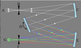
To figure out the spectral response of the detector, we use a monochomator and photodiode for which we know the spectral response. As a quick review, a monochromator transmits a selectable narrow band of wavelengths of light that the operator selects. The use of a calibrated photodiode allows the measurement of sensor irradiance, the power per unit area of radiant energy falling on the sensor.
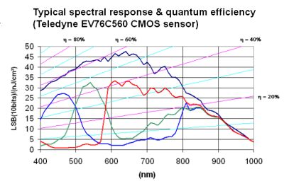
Sensor chip makers publish the spectral response of their devices, usually given as a plot of output level for 1 nJ/cm2 input vs. wavelength in nanometers. Monochromator readings can be compared to the published levels to verify the sensor response.
Finally, we should mention a new kind of image sensor, the Quanta image sensor (QIS). The QIS computes an image by literally counting photoelectrons over space and time. The QIS consists of specialized pixels called jots. Their full-well capacity (the number of charge carriers they generate before they saturate) amounts to just a few electrons and they don’t use avalanche multiplication.
The QIS may contain hundreds of millions or possibly billions of jots read out at speeds of perhaps 1,000 fps or higher, implying raw data rates approaching 1 Tbit/sec. Through use of advanced denoising algorithms, good grayscale images can be captured in extreme low light of less than one photon per pixel on average.
Ordinary CCD and CMOS image sensors integrate received photocharges and digitize them. Their full-well capacity defines the upper end of their dynamic range, while read noise defines the lower end. A problem on the low end is that the photoavalanche process these sensors use causes problems in low light such as a variance in the charge gain. They are also sensitive to silicon defects, leading to high dark charge carrier count rates that limit low-light performance and manufacturing yield.
On the other hand, in a QIS photon-counting image sensor forms an image pixel computationally from a series of jot values registered over time and within a defined space. While QIS images one photon at a time, it can still realize a high dynamic range (>120 dB) using special multiple high-speed exposures.


Leave a Reply
You must be logged in to post a comment.