If transistor circuits are to be of any use or amenable to diagnostic procedures, we must be able to model them. Even the best electronic test equipment is useless if we don’t know what to look for in the circuits under investigation.
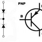
Transistors characteristically have multiple modes of conduction. We can view these phenomena in the two-diode model of a bipolar junction transistor (BJT). Two diodes whose anodes join to form a center tap are analogous to an NPN transistor insofar as ohmmeter readings accurately represent the real device. Two diodes with cathodes connected to a common node are analogous to a PNP transistor. (NPN transistors are preferred due to increased mobility of electrons compared to holes and also because they are compatible with a negative ground system.) Because two diodes are separate components and cannot share in common a semiconducting layer, they do not function as an amplifier, go into oscillation or perform switching action in the manner of actual transistors.

To accurately model a BJT, we must look beyond the simple diode hookup, although that remains relevant. The Ebers-Moll Model is an electronic representation of a transistor, either NPN or PNP, in any of the four fundamental configurations. In addition to the diode model, which is a physical simulation, Ebers-Moll is a paper construct, having its existence in part as a schematic diagram and also a set of equations, either of these deploying conventional symbols.
Jewel James Ebers and John L. Moll introduced this mathematical model of transistor currents in 1954. The model is described in a paper titled Large Signal Behavior of Junction Transistors, which appeared in Proceedings of the Institute of Radio Engineers. In the paper’s Abstract, the authors say:
In the consideration of the junction transistor as a switch there are three characteristics of primary interest, the open impedance, the closed impedance, and the switching-time. A generalized two-terminal-pair theory of junction transistors is presented which is applicable, on a dc basis, in all regions of operation. Using this theory, the open and closed impedances of the transistor switch are expressible in terms of easily measurable transistor parameters. For the ideal transistor, these parameters are the saturation currents of the emitter and collector junctions and the normal and inverted alphas. The transition of the transistor switch from open to closed, or vice versa, is discussed, including the effects of minority carrier storage. This transition can be expressed in analytic form in terms of the alphas and the normal and inverted alpha cut-off frequencies.
The Ebers-Moll Model consists of these equations for emitter and collector current:

Forward and reverse gain, denoted by αF and αR, are less than one because not all current finds its way from one junction to the other.
This reciprocity condition, as it is known, implies a base current that can be calculated using Kirchhoff’s Current Law, according to which the sum of all currents entering the node is equal to zero. Notice that
In the BJT, typically there are two two-wire circuits, input and output. The device in its fundamental form has three rather than four terminals because one of them — which can be base, emitter or collector — is common to both circuits. The output circuit can convey to the next stage an amplified or an attenuated version of the signal at the input. When the input and output at each point in time are in the same ratio, the device is said to be linear and when that ratio varies, the device is non-linear.
X = 2Y is a linear equation.
X = Y2 is a non-linear equation.
Both linear and non-linear devices possess some finite gain. Or gain can be infinite, theoretically but not in actuality, where a big-bang condition would exist. Gain is denoted by Greek alpha (α) and Greek beta (β). To clarify, α is IC/IE. β is IC/IB. The common-emitter voltage gain is always in low negative territory.
The current gain in a common base transistor circuit is by definition the change in collector current over the change in emitter current when the voltage difference between base and collector does not vary. A typical common base current gain is one.
In a BJT, each of the two junctions can be forward biased or reverse biased. Accordingly, there are four possible modes in which the transistor can operate. It is cut off when the emitter-base junction and the collector-base junction are reverse biased. When both of these junctions are forward biased, the device is in saturation. When the emitter-base junction is forward biased and the collector-base junction is reverse biased, the transistor is in the forward-active mode. Finally, the transistor is in the reverse-active mode when the emitter-base is reverse biased and the collector-base is forward biased.
Between cutoff and saturation, the device acts as a switch, which may be open with a high impedance or closed with a low impedance. In these biasing conditions, there is no intermediate state. In the forward-active mode, the transistor operates as an amplifier, and in the reverse active mode, it may be used in digital and analog switching operations.
Surprisingly, under certain biasing and signal input conditions, the physical dimensions of a BJT will actually change. This phenomenon was first noted by James Early in 1952 and is known as the Early effect. It manifests as a shrinking base width due to a widening of the base-collector depletion region. The result is a rise in collector current and voltage. Metal-oxide semiconductor field-effect transistors (MOSFETs) also exhibit this strange behavior.
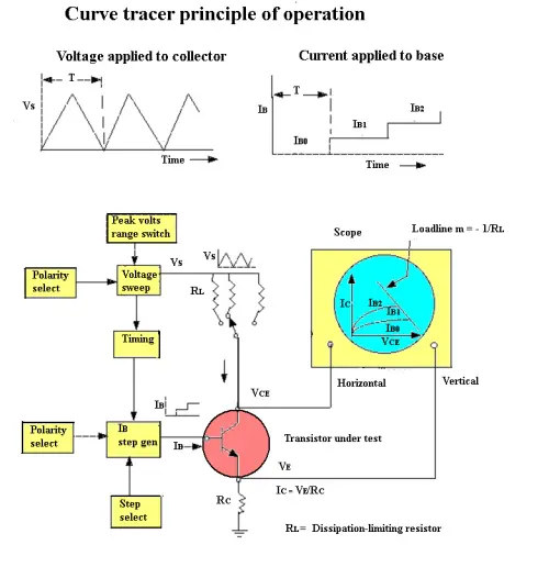
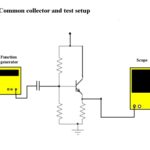
When it becomes necessary to physically measure transistor parameters such as current gain, breakdown voltages, and impedance, a transistor curve tracer is usually the instrument of choice. The curve tracer can generate and display a family of curves of collector current, Ic, versus collector-to-emitter voltage, VCE, for various values of base current, IB. From this display, the current gain, β, can be directly determined.
A curve tracer uses three basic circuits to generate this display: a sweep-voltage-generator for control of the collector voltage; a base current source which can be controlled to provide a number of equal increments of base currents with each sweep of the voltage generator; and a timing source to change the base current at the start of each voltage sweep.
The waveform of the sweep-voltage generator, Vs consists of repetitive sweeps occurring with a time period T. This is the collector supply voltage which is repetitively applied to the transistor. The collector voltage, Vce, will provide the horizontal (x-axis) sweep.
A view of the output of the base current source shows that for each consecutive voltage sweep the base current, IB, is incremented in equal steps with each step synchronized to the beginning of each collector voltage sweep. As the last increment period ends, the base current generator repeats the step sequence. In the U.S., the 60 Hz power line frequency is generally used as the synchronizing signal for the collector sweep voltage and base current steps.
The collector-to-emitter voltage, Vce, provides the horizontal sweep, while the voltage across the current sensing resistor, Rc, which is proportional to collector current, provides the vertical sweep, resulting in a family of curves of Ic versus Vce for a series of equal increment changes in base current.
The displays shown here are for an npn transistor. The current gain of the transistor is determined from: β = current gain = ΔIc/ΔIB where ΔIB is set by the curve-tracer Step Selector switch.

The slope of the load line is determined by a dissipation-limiting resistor, RL, selected in the collector sweep control section. This resistor is selected so the maximum allowable collector current, Ic, for the transistor is not exceeded for Vce = 0 V.
When put on a curve tracer, small transistors don’t have much heat dissipation capability so they should be limited to about 50 mA and 40 V; higher power transistors usually have a case that permits attachment to a heat sink. It’s usually safe to assume they can handle 1 or 2 A at 40 V.

β will vary depending on the collector current drawn, dropping as the current rises. The gain is generally measured in the voltage/current region in which the transistor is expected to operate.
Finally, transistors on a curve tracer can heat up, so use caution in handling them.

Leave a Reply
You must be logged in to post a comment.