There are three bipolar junction transistor amplifier topologies: common emitter, common base and common collector. (For field-effect transistors, the analogous circuit configurations are common source, common gate and common drain. In the old world of vacuum tubes, they were common cathode, common grid and common plate.) This particular classification derives from the external circuit configuration.
 An emitter follower circuit, also known as a common-collector amplifier, is the quintessential negative feedback device. What’s good about it is its high input impedance, which has the effect of not loading, i.e. being virtually invisible, to the previous circuit. Moreover, the output impedance is low, so it is not destabilized by the following circuit if that happens to be a heavy load. In other words, the transistor is a robust voltage buffer.
In the common collector arrangement, the input voltage is applied between base and collector, and the output voltage comes from the differential that exists between emitter and collector circuits. Because the emitter voltage is a function of the input difference, the device is usually called an emitter follower.
The circuit is characterized by two important attributes: The gain is close to unity at all times, regardless of changes in bias, individual manufacturing variations, thermal effects, loading in a subsequent stage or value of any collector resistor. And second, the output is the inverse of the input. This is not at all a disadvantage, provided it is taken into account. If there is an even number of stages, the overall output is not inverted.
In an emitter follower amplifier circuit, the output in addition to being inverted, is just a little less than one because the emitter voltage is pegged at the diode drop of about 0.6 V below the base. Because there is no voltage amplification in this circuit, one may wonder if it has a purpose. The answer is that its value lies in the fact that its input impedance is far greater than its output impedance. Accordingly, less power is required from the input to drive the output if there were a straight-through connection rather than the emitter follower circuit. For this reason, an emitter follower has current gain. Because voltage gain is close to one, the circuit has substantial power gain. The small output impedance of the emitter follower reduces any loading of the subsequent stage.
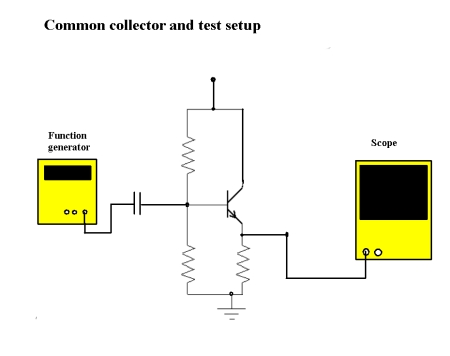
Oscilloscopes can be useful in displaying some of the qualities that emitter followers exhibit. If the amplifier is fed from a waveform generator, apply both the amplifier output and the waveform generator output to separate channels of the scope. The inverted nature of the amplifier output should be evident from the scope display. So, too, should be the fact that there is no voltage gain in the output.
Similarly, it should be easy to see the amplifier frequency response on the scope display. We adjust the output frequency of the waveform generator until the output of the amplifier falls to 70.7% of its normal output. This is the 3 dB rolloff point. It is easy to note this point by setting voltage cursors on the scope to the 70.7% point.
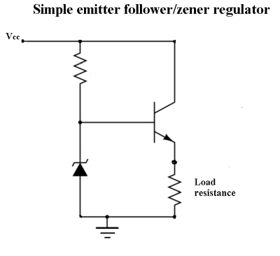 One application of the emitter follower amplifier circuit is as part of a voltage regulator, taking advantage of its capability as a buffer. In some non-critical circuits where the supply current never rises above a specified level, a simple zener diode will do. But there are problems in this bare-bones voltage regulator because the output cannot be adjusted or set. The zener’s non-destructive reverse bias breakdown merely cuts off voltage above a certain level based on choice of the diode. Additionally, because of limited dynamic impedance, zeners provide minimal ripple rejection and stability in the face of input and load variations. When loading is subject to large variation, only a high-power, expensive zener can cope with elevated heat dissipation. Here again the emitter follower amplifier is an effective remedy.
To isolate the zener, an emitter follower along with a resistor can be placed in series with the output to limit current. This is done through a collector resistor so a voltage divider is formed with the zener diode reverse-biased from the voltage divider center-tap to ground. The center point of this voltage divider can be brought to ground through a capacitor connected to the added center tap. This added component effectively reduces ripple.
Like any current source (battery, generator), an emitter follower can transfer power to its connected load only up to a finite voltage level. The voltage range without current drop-off is known as its output compliance. This is equivalent to saying that in the case of an emitter follower it must remain within its active region. The collector voltage must range from near saturation up to the maximum possible, the supply voltage, unless the load contains an additional power source.

This is very unique and interesting information. Thanks for sharing this with us. Kindly post more informative content like this.
It’s very useful content. Many electronics student don’t know how to find base, emitter, collector of the resistor. Thanks for your nice efforts. Now i know how to test base, emitter, collector
A rare insight into the applications of a transistor and its configurations.