In digital electronics, jitter is a particularly insidious form of noise, to be understood, measured and where possible mitigated. Jitter is short-term, generally considered less that one second, deviation from the design intent. It consists of timing fluctuation in periods or transitions within cycles.
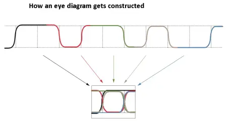
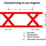
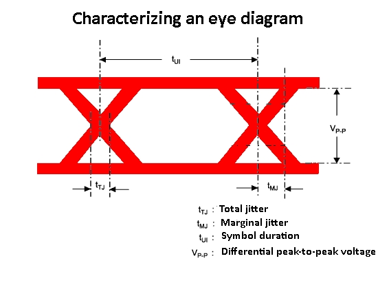 An eye diagram tells the whole story. While vertical closing of the eye reveals fluctuations in signal amplitude, a horizontal narrowing indicates timing, period or cycle error, a definition of jitter.
It is not a hard and fast distinction, but generally 10 Hz is considered the boundary between slower frequency variations, known a wander, and faster frequency variations, known as jitter. Jitter consists, among other things, of peak-to-peak displacement of a time varying signal. The signal amplitude is changing at a rate that is either slower or faster for a given frequency context, so its value at any point in time will be uncertain, if there is jitter. In digital electronics, where there is a decision threshold, jitter can prevent logic 0 and logic 1 at the output from coinciding in time with their states at the input. This is the unfortunate consequence of jitter. It is the task of the engineer or technician to quantify this jitter, discover its cause and take steps to mitigate it.
Often what we are looking at is jitter in the clock signal coming from a square-wave oscillator. This jitter can be caused by thermal noise, loading status, power supply fluctuations, device noise or interference from adjacent circuitry. One or more of these factors in concert can give rise to jitter. Methods for measuring jitter depend upon its type, which may be period jitter (cycle-to-cycle or otherwise), long-term jitter, phase jitter and time-interval jitter.
 Period jitter is defined as difference in cycle time compared to the design period. It is cumulative and therefore becomes pronounced over multiple cycles. To measure period jitter, the procedure is to measure the duration of one clock cycle, rising edge to rising edge. Then, after some number of cycles, repeat the measurement.
Cycle-to-cycle jitter is defined as the variation in cycle time between adjacent cycles. Since cycle-to-cycle jitter is applicable to variation between adjacent cycles, it has nothing to do with an ideal cycle. To measure cycle-to-cycle jitter, record the durations of two adjacent cycles. After a number of these cycles, repeat the measurement. Following numerous measurements, the largest number can be taken as a peak value.
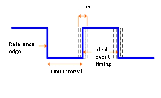 Long-term jitter, in reference to a clock output, is its change from the ideal position over adjacent cycles. It differs from period and cycle-to-cycle jitter in that it is applicable to the cumulative effect of jitter in the course of many clock cycles.
To measure long-term jitter, it is necessary to measure the time intervals of numerous clock signals. Then, after more clock signals, repeat the measurement. Do this a great many times, computing mean, standard deviation and peak-to-peak values. After a number or repetitions, the average peak-to-peak value can be computed.
Phase jitter consists of noise values at either divergent phase offsets from the ideal or as continuous noise over a range of frequencies. If we integrate these values, i.e. multiply them by time, we arrive at a phase jitter metric over a specified spectrum, given in seconds.
In a clock signal we are dealing with a square wave, so most of the energy resides at the center frequency. Portions of this energy, however, appear above and below the center frequency. Phase jitter is equivalent to the amount of phase noise that exists between two of the offset frequencies.
Phase noise can be quantified by looking at the frequency domain display and measuring the areas of the sidebands below the plotted trace.
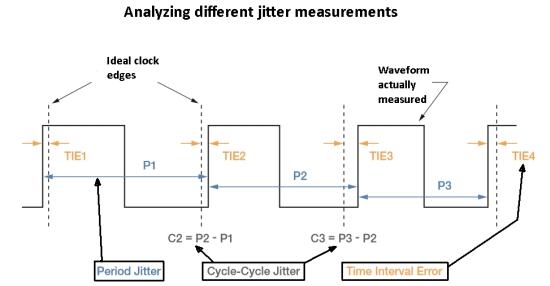 Time interval error is the time deviation of a rising edge from the ideal or, when the ideal is not available, the deviation between the rising edge and an observed average value. To detect and quantify jitter, and correlate it to a time-varying cause such as anomalies in a power supply, the investigator will use one or more of these test instruments:
• A bit error rate (BER) tester sends a pseudo-random bit sequence (PRBS) through a system or device that is being tested. The instrument then compares each bit in the data stream against the PRBS, and a BER is calculated. The computation is absolutely accurate, but the procedure is time-consuming, sometimes requiring many hours. Testing time can be greatly reduced when a BERT scan is performed, using statistical techniques.
• Jitter analyzers, variously called timing-interval analyzers and signal-integrity analyzers, are capable of measuring jitter in a clock signal. Jitter characteristics are measured and the bit error rate is calculated more quickly than in the BER tester. The jitter analyzer measures the time interval between signal edges and applies algorithms, generating histograms, frequency displays and other relevant graphics. Using these tools, the instrument resolves total jitter into subspecies, random and deterministic jitter.
• Oscilloscopes — with time and frequency domains, math mode, multiple analog and digital channels, etc. — are often the tools of choice in jitter measurements. A real-time oscilloscope is capable of testing devices, media and entire communications systems that convey data at maximum copper speed, where it tops out at a little over 3 Gbits/sec. These instruments can see jitter in clock signals including but not limited to those used in communications. A high-bandwidth sampling oscilloscope such as the Tektronix CSA8000B Communications Signal Analyzer generates measurement results with time and amplitude histograms, mask testing and statistical results. It includes noise, duty cycle, overshoot, undershoot, extinction ratio, Q-factor, mean optical power, amplitude measurements and jitter.
In an oscilloscope, the user can create eye diagrams by setting the persistence at infinite. Repetitive signals such as PRBS patterns are needed. The major oscilloscope manufacturers make available jitter analysis software. In this respect the oscilloscope resembles a jitter analyzer. A single screen simultaneously displays timing error of discrete bits, referring to an ideal clock generated in the software. Additionally, there is an instantaneous phase plot of the data stream. An FFT display of the timing error plot shows the jitter frequency. The user can compare this metric to the clock frequency of a power supply or isolate the problem to crosstalk in the system’s data media.
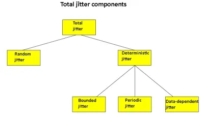
In regard to ascertaining the cause(s) of observed jitter with a view to mitigating it, the first step is to understand the difference between random jitter and deterministic jitter. Random jitter has a gaussian distribution while deterministic jitter is non-gaussian. Random jitter is unbounded. One cause is thermal effects in semiconductors. It is a consequence of vertical noise in a system, which if its magnitude is sufficient will result in random timing error, or jitter.
Deterministic jitter is unbounded. It is revealed by measuring and comparing peak-to-peak values. One pathology is duty-cycle distortion, which is a cause of logic level errors.
Bandwidth limitations in the transmitter or media are causes of inter-symbol interference, also known as data dependent jitter. Under these conditions, limited rise and fall times in the signal result in data bit amplitude irregularities. If the decision threshold is compromised, logic levels can become garbled. Improper impedance terminations will do the same thing, due to reflections and harmful data collisions. All of this becomes more critical at higher frequencies.
Periodic jitter is caused by cross coupling or excessive EMI, and it sometimes but not always is correlated to the original data signal. A prime offender in uncorrelated periodic jitter is a switching power supply, where the EMI is caused by fast voltage transitions.
One method for reducing EMI is by installing bypass capacitors across the input or output power and return lines. Additionally, a pair of coupled inductors can be placed in series with each power conductor. Another method for reducing EMI is to place the noise-generating circuitry inside a grounded metal enclosure. A related mitigation measure is to run all signal-carrying media in a grounded metal raceway. The metal conduit or tubing should be bonded at both ends (by the usual mechanical terminations) to the respective metal enclosures, which are tied to the premises electrical system ground. This is opposed to literally running a “ground wire” to the earth.


Leave a Reply
You must be logged in to post a comment.