The Applied Science YouTube channel run by Ben Krasnow (who in his day job is a hardware engineer at Verily, Google Life Sciences) focuses on interesting applications of science and technology. One video in particular caught our eye where Kranow uses an oscilloscope to help view digital images captured by a scanning electron microscope made by Jeol BV in the Netherlands.
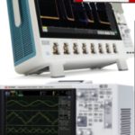
Specifically, Krasnow uses a DSO having a long record length to capture details of SEM scans that last ten seconds or more. This is an interesting idea that potentially has application in other areas characterized by relatively long capture times. Krasnow used a Tektronix MDO3104 scope but the capture modes he employed can be found on many modern scopes. So we’ll review Krasnow’s approach here.
Krasnow’s SEM is an old device rescued from the trash. To capture images, the user normally attaches a Polaroid camera to an adapter and then holds the shutter open to capture a single frame from the SEM display. To get a high-resolution SEM image, it can take up to 60 seconds for the electron beam to scan across the sample. The reason for the long scan time is that electron microscopes work by focusing a beam of electrons onto the sample and then measuring the amount of emitted electrons reflecting back. High-rez images require that only a relative few accelerated electrons be beamed at and be reflected from the sample. So it takes a while for enough electrons to be accumulated to form any kind of an image.
Krasnow had the idea of using an oscilloscope with a sufficiently long record length to take the place of the Polaroid camera in recording images. What made this approach feasible was the availability schematics for the SEM. Krasnow probed the SEM PCB until he found the point where the video signal for slow scans was available. Also helpful was that the scan readout signal was on the order of about 90 V. He fed this signal to one scope channel. Krasnow also found a horizontal sync pulse which he used as a trigger. The data coming between each sync pulse represented one line of video. This setup produced a scope display that changed in shape and intensity as the SEM scan moved from the top of the screen to the bottom.
After maximizing the waveform on the DSO display to fill the entire screen, Krasnow changed the sampling mode to high resolution. The high-resolution mode on modern scopes basically performs averaging on the samples to effectively lower the noise floor. To get an image containing at least one megapixels, Krasnow chose a record length of five million. He used a vertical sync pulse (which happened once every 10 sec) as a trigger (with the scope in normal trigger mode) so that when the SEM starts a scan, the display triggers at the right point. Moreover, he used a pulse-width trigger so the display triggers when the pulse was greater than 500 μsec.
Krasnow also had to adjust the scope horizontal scale to capture the scan in one block. He used a 2 sec/div horizontal scale to fit one entire scan onto the scope screen.
Once the scope triggers, it takes a while for a display to appear. The reason is that in the normal trigger mode with capture rates on the order of 250k samples/sec, the scope doesn’t display anything as data gets acquired. Once the scope has recorded a whole video frame, the image really isn’t in a form that looks like a conventional SEM display. To clean things up, the frame can be saved as a file and loaded into a PC for some clean up. On Tek scopes, you can set cursors on the screen to select the portion of the display you want saved to a file.
For the clean-up, Krasnow used a program called Octave, which basically an open-source version of the Matlab analytics program. He wrote a script that put individual scan lines together to assemble an image raster-scan style. The result was a good rendition of the MEMS gyroscope target. There was a slight distortion that arose because Krasnow picked the signal off the SEM circuit board, slightly changing the portion of the target being imaged.
All in all, an interesting use of a scope’s ability to capture lengthy time periods.


Leave a Reply
You must be logged in to post a comment.