The two major types of power supplies, linear and switch mode (SMPS), operate according to entirely different principles and have distinguishing characteristics. Design work and maintenance on each one requires totally different mindsets.
The SMPS is now widely used because of its greater efficiency, lower cost and better weight and thermal qualities. There are some disadvantages, which however can be mitigated by careful planning in the design stage.
First, by way of perspective, we’ll revisit the old linear power supply. It was a familiar part of analog CRT TVs, contributing to the considerable weight because of the heavy power transformer. This was a plus, however, because multiple secondary taps made available any number of voltages, as needed for bias, filaments, picture tube deflection, etc.
In linear power supplies, the active devices operate in the linear portion of their response curves. This is in contrast to the SMPS, where first the input power is converted to square waves of varying duty cycle. The active components operate in non-linear modes. When components operate in linear portions of their response curves, they effectively act like variable resistors that dissipate power (because of I2R). This is why a considerable amount of the input power is dissipated in the form of heat, and this is the situation in a linear power supply.
The linear power supply consists of a series of stages. The ac line, often starting with a plug to pick up 120-V, single-phase utility power, passes through a grommeted opening in the cabinet where, at the point of entry, there is always a fuse and switch with optional power light. It feeds the primary of the power transformer, which may have any number of secondary windings. Besides the capability of providing a number of voltages, this type of transformer has no electrical connection between primary and secondary windings, so it is known as an isolation transformer. (Grounding does not pass through a transformer unless it is an autotransformer, where primary and secondary are a single winding, tapped at different points.)
What’s good about the linear power supply is that the power flow is easy to follow. It goes to the rectifier, consisting of one or more diodes, to electrolytic filtering capacitors, parallel-connected to remove ac ripple, and occasionally to more expensive series-connected inductors to further purify the dc. Then comes a linear regulator and final dc output. It is all easy to design and diagnose. The most common troublemakers are the electrolytic capacitors, which can be visually inspected and checked with a multimeter.
As mentioned before, the semiconductors in a linear supply can effectively form a large resistance that dissipates heat, and linear supplies incorporate bulky components (such as the transformer) that make the supply physically large. For small consumer appliances, the heat may not be an issue but the larger component sizes and weight might be. Cell phones and laptops as we know them would not be possible with linear power supplies.
In contrast, an SMPS incorporates a transistor that operates as a digital switch. The switch is either off, conducting virtually no current, or fully on, with little resistance. The only time heat is generated and must be dissipated is during the on/off transitions. The extremely fast rise and fall times of the square wave make these transitions vanishingly brief. This factor accounts for the great efficiency of the SMPS. Furthermore, as we shall see, the isolation transformer operates at the switching frequency, so it can be smaller compared to the 60-Hz power line transformer that is an essential part of the linear power supply.
 Small component size, greater efficiency and lower cost have resulted in widespread use of the SMPS in nearly all electronic equipment. Recent innovations have permitted its use in high-power applications. But SMPS implementation has not been totally free of problems. One of these is the generation of electronic noise, which if not mitigated can appear at both the input and output of the SMPS. In addition, electronic noise generated by the switching process can propagate as radiation from the device. This is because the square wave, with its near instantaneous rise and fall times, resembles a high-frequency energy source rich in damaging harmonics.
When powered on, the SMPS exhibits inrush current, which can affect nearby sensitive equipment through the power distribution system. Another potential problem caused by harmonics is the heating of the neutral conductor in the power supply. The solution is to oversize this wire. Generally speaking, even where refinements are required, the overall benefits in SMPS are significant regardless of scaling.
Voltage regulation is an integral part of the SMPS. It works by varying the ratio between on time and off time. This technique is a decisive advance over the linear power supply, where output voltage has to be dissipated in the semiconductor.
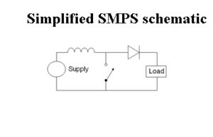
The SMPS output is a function of its input, but not according to the ratio of primary and secondary turns in the power transformer, as in a linear supply. In contrast, one configuration that is typical in an SMPS is to have a dc voltage in series with an inductor and switch, driven by a square wave. Measured across the switch, the peak-to-peak voltage can exceed the dc voltage as measured at the input. This is one of the reasons that SMPS work is not for the faint-hearted.
The higher voltage comes about because the inductor creates an induced voltage in response to changes in current. This voltage is added to the dc source voltage during the period of time that the switch is open. A further refinement is to add a diode and a capacitor to the switch. The peak voltage will be stored in the capacitor in the form of an electrical charge. At this point, the capacitor becomes a dc source and the overall output voltage becomes greater than the dc voltage at the input. This is a boost converter that works on dc, not ac. It is the switch-mode equivalent to the step-up transformer in a linear supply.
Still another switch-mode variation is a buck-boost converter that changes the polarity of the output with respect to the input. Another implementation is a buck circuit that boosts average output current, the price paid being a lower output voltage.
There are many variables in how an SMPS is configured. The output current flow is always a function of the input power. But with numerous circuit topologies and various methods for driving the switch — such as pulse width modulation — there are endless combinations. Thus there is a far steeper learning curve compared to the linear power supply.
The chief difficulty when making measurements of an SMPS is that often the waveform of interest is a millivolt-level ripple sitting on top of a signal in the 100-V range. Similarly, components in the supply can operate at about 100 V in one state and at millivolts at another. This kind of big dynamic range can pose a problem for the eight-bit digitizing scopes common in electronics labs.
For example, one common SMPS measurement is to determine switching loss and average power loss across the switching device. The first step is to determine the voltage across the switching device during the off and on times. The voltage across the switching device has a high dynamic range. The voltage across the switching device during the on state depends upon the type of switching device. The off-state voltage depends on the operating input voltage and the supply topology. At maximum input voltage for an SMPS with a 120-V input, the off-state voltage across the switching device can be as high as 750 V. During the on state,
the voltage across the same terminals can range from a few millivolts to about one volt.
To capture such signals, the oscilloscope vertical range would be set at 100 V/div. At this setting, many scopes will accept voltages up to 1 kV. The problem with using this setting is that the minimum signal amplitude an eight-bit scope can resolve is 1,000/256, or about 4 V.
Some modern scopes offer power application software that addresses the issue by letting the user enter RDSON or VCEsat values for the main semiconductor switch from the device data sheet, rather than trying to measure them directly. Alternatively, if the measured voltage is within the scope sensitivity, the application software can use acquired data for its calculations rather than values entered manually.
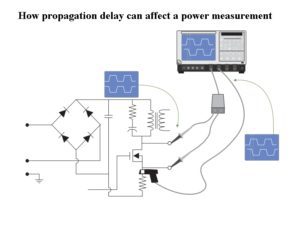
Another issue that arises in SMPS measurements concerns the use of voltage and current probes. It is necessary to measure voltage across and current through the switching device, either a MOSFET or a bipolar transistor (usually an IGBT). The task requires two separate probes: a high-voltage differential probe and a current probe. Each of these probes has a different propagation delay. The difference in these two delays, known
as skew, causes inaccurate timing measurements and distortions in the displayed power waveforms.
Probe propagation delays can impact maximum peak power measurements simply because power is the product of voltage and current. If the two multiplied variables are not perfectly time aligned, the result will be wrong.
Fortunately, there are ways to deskew the probe readings so the accuracy of measurements such as switching loss doesn’t suffer. Some power measurement software will automatically de-skew the probes. Here the software takes control of the oscilloscope and adjusts the delay between the voltage and current channels using live current and voltage signals.
Also available is a static de-skew function. This function uses the fact that certain voltage and current probes have constant and repeatable propagation delays. An embedded table of propagation times for selected probes lets the static de-skew function automatically adjust the delay between selected voltage and current channels.
Differential and current probes may have slight offsets that should be removed before taking measurements. Some probes have a built-in, automated method for removing the offset. Other probes require manual offset removal. Most differential voltage probes have built-in dc offset trim controls, which makes offset removal relatively simple.
Similarly, current probes need adjustment before making measurements. Differential and current probes are active devices, and there will always be some low-level noise present, even in the quiescent state. This noise can degrade measurements that rely on both voltage and current waveform data. Consequently, some power measurement software includes signal conditioning features that minimize the impact of inherent probe noise.
Finally, there is the whole matter of power factor, which is a concern of the facility manager as well as the utility. A linear power supply typically has low power factor. An SMPS that does not have power factor correction draws a large amount of current coinciding with the ac waveform peaks. This problem can be mitigated with well-designed power factor correction. Similarly, the heavy inrush current in an SMPS can be mitigated by soft-start equipment.
To summarize, compared to a linear power supply, the SMPS is efficient and low cost. However, its far greater complexity necessitates expertise that goes beyond simple electronics.

Wow! Very informative. I now see why my multimeter doesn’t measure anything when I try to measure the output voltage of the switching power supply! Thanks!