by Mike Borsch and Mike Schnecker, ROHDE & SCHWARZ
Modern transceivers often incorporate several parallel RF front ends whose control signaling can be sorted out with advanced instrumentation.
The radio frequency (RF) front-end configuration in mobile devices continues to evolve and get better. The trend in mobile radio communications is toward complex multi-radio systems perhaps incorporating several parallel transceivers. This makes modern RF front-end design super complex.
The Mobile Industry Processor Interface (MIPI) Alliance Specification for RF Front-End Control Interface (RFFE) is widely used within wireless devices to more efficiently control these complicated front ends. The interface boosts performance by supporting multi-mode, multi-band and multiple antennas, all with a minimum number of wires and pins using a single RFFE bus.
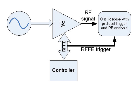
One key function of the RFFE interface is controlling the power amplifier gain as well as switching the RF signal. It’s critical to understand the reaction time and characteristics of the signal in relation to the specific RFFE command. And it’s vital to test RFFE command synchronization for power amplifiers. A measurement system must trigger on an RFFE protocol event, measure the RF power envelope of the signal, and analyze the spectrum. Oscilloscopes use a combination of features –including spectrum analysis and RMS detection, along with real-time serial data trigger and decode — which make them well suited for this measurement.
RFFE background
The RFFE interface is designed to support existing Third Generation Partnership Project (3GPP) cellular standards such as LTE, E-GPRS, UMTS and HSPA, as well as non-3GPP air interfaces. It is intended to be efficient, flexible, and extensible, accommodating many variations in the overlying system design. Simultaneously, it provides interoperability at the interface level between compliant radio frequency integrated circuits (RFICs) and front-end modules (FEMs).
There are a variety of FEMs, including power amplifiers (PAs), low-noise amplifiers (LNAs), filters, switches, power management modules, antenna tuners and sensors. They may reside either in dedicated devices or be integrated into a single device, depending on the application and technology applied.
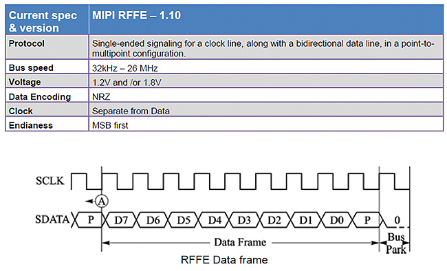
To control RF devices, RFFE has requirements for both the physical and upper protocol layers. It incorporates a compact two-wire interface (SCLK, SDATA) with one master clock that can go up to 26 MHz. Data transfer bidirectionally among up to 15 slave devices per bus master. One specialty of the protocol is that the SDATA receiver may use a glitch rejection filter on the SDATA input.
The latest version of MIPI RFFE, v2.0, brings five important technical features to the widely used interface. First, it provides for an extended range of bus operating frequencies that effectively doubles the number of command sequences that can transfer on the bus in a given amount of time. This feature boosts overall data speeds for end users. Second, a synchronous read lets the slave devices propagate more types of data on the bus to expand the range of bus loading and enable the use of extended frequencies. Third, a multi-master configuration supports carrier aggregation system architectures as well as the use of multiple transceivers and dual-SIM designs. Fourth, an interrupt-capable slave function gives the master controller on the bus a quick way to poll the slave devices. Finally, reserved registers improve the efficiency of hardware and software development.
A typical RFFE measurement is the settling time for a PA after a gain shift. The controller issues an RFFE command to the PA which, in turn, adjusts its gain accordingly. The key measurement is the time from the receipt of the command to where the power settles to within a percentage of its final power level. This is a function of the amount of gain adjustment (larger is more difficult) as well as several other conditions such as the frequency of the signal.
Most serial bus architectures rely on the concept of abstraction layers or a protocol stack to transmit information using fewer physical lines. Because an oscilloscope captures the analog information (physical layer), it often contains the root information for viewing protocols as well.
RFFE protocol trigger
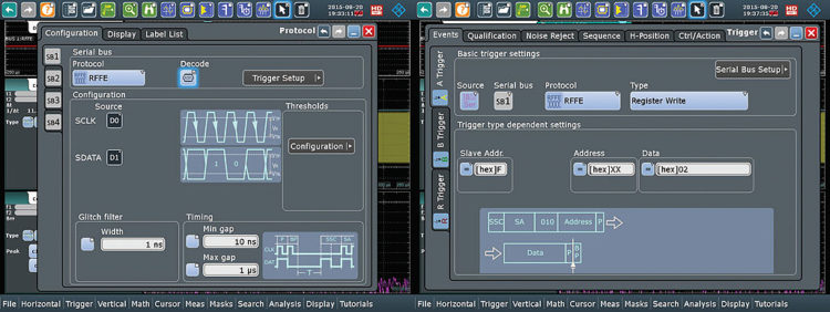
One benefit of oscilloscopes is their ability to trigger on specific signal qualities to allow capturing and measuring specific portions of a signal. Modern oscilloscopes can trigger on a wide variety of signal events from a simple edge to more complex features such as pulse width and slew rate. Going one step further, some oscilloscopes can interpret a given signal as a serial data stream, detect the bits, and then interpret the protocol using this stream as a trigger event.
Many digital scopes allow glitch detection. This is an important feature that, in the case of the RFFE interface, prevents erroneous detection of logic levels on noise. The decoded signal is displayed time-aligned with the analog signal. Once defined, the serial bus can be used as a trigger source and trigger defined events.
Numerous techniques have been used to measure the power of a signal. Peak power meters are the most accurate way to measure the power level. But these meters do not have an RFFE triggering capability, so they can’t make timing measurements.
A common way of detecting signal power is to use a detector. A detector is basically a diode that converts the RF carrier to a voltage proportional to the square of the signal amplitude. The detector voltage is then displayed on a scope.
While the square-law detector is effective, it is also possible to use math on the acquired waveform to realize the square-law detection. High bandwidth oscilloscopes, such as the Rohde & Schwarz RTO, use fast A/D converters to acquire the signal waveform at RF (in the case of the RTO, this sampling rate is 10 Gs/sec). The power envelope changes at a much lower rate than the carrier. So the sample rate of the A/D can be lowered using a process called decimation which drops samples.
The decimation process can also take place using math. By computing the RMS value of the signal over a specific interval, say 100 samples, the sampling rate drops to 100 Ms/sec and the waveform is equal to the RMS voltage of the RF signal. The power is displayed by scaling the waveform, dividing it by the 50-Ω input impedance of the oscilloscope.
Spectrum measurement
It is often useful to know the spectrum of the RF signal during switching. That’s because it is undesirable to generate out-of-band spurious signals that can interfere with other receivers in today’s dense RF environment.
Oscilloscopes measure the RF spectrum by running a fast Fourier transform (FFT) algorithm on the acquired signal. Here the spectrum represents a “snapshot” in time of the frequencies present, synchronized with the other signals being measured on the oscilloscope, including the RFFE bus. A technique called FFT gating can be used to focus the spectrum measurement on a specific time within the acquisition identified by a gate.
Some oscilloscopes, like the R&S RTO, include a fairly subtle but significant FFT capability. Standard oscilloscopes compute the FFT on a portion of the signal waveform determined by the desired frequency resolution. For example, a 100-kHz-resolution bandwidth requires an acquisition time of 10 µsec (actually 20 µsec because of windowing). If the acquisition time necessary for the switching event is, say, one millisecond, only 10% of the waveform is used. In many cases, the oscilloscope will force the FFT to use all of the waveform data, thereby setting the resolution to 1 kHz in this case.
This resolution issue causes problems: The computation includes 10x the number of data samples, and it is not possible to gate the time over which the spectrum is computed. More advanced oscilloscopes let users set the resolution independent of the displayed waveform time. If more time is available, then the scope computes multiple FFTs on subsections of the waveform, and the displayed spectrum is the overlay of them all.
All in all, the interface of the RTO oscilloscope offers a time-accurate triggering mechanism that enables precise control of time-critical functions in multiple slave devices. The specification also controls a variety of command sequences that can be used to determine the amount of data that can be transferred on the bus, and employs slew-rate controls to help mitigate emissions at sensitive radio receivers.
An oscilloscope with RF measurement capabilities and serial trigger and decode can help accurately measure the response time and power spectrum of MIPI RFFE signals and contribute to a better user experience.
MEASUREMENT EXAMPLE
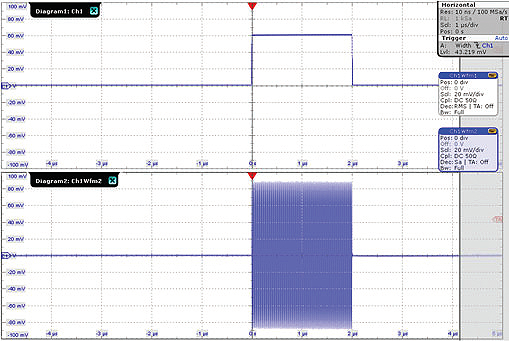
Suppose the device-under-test is a PA controlled by an RFFE signal, and the power is ramped by switching on the PA. A Rohde & Schwarz RTO1044 oscilloscope is set to probe the RFFE clock and data lines using digital signal lines D0 and D1 respectively on the MSO module. The PA is commanded to switch on and the oscilloscope is set to trigger when the data value 0x02 hex goes to slave address 0xF on the RFFE bus.
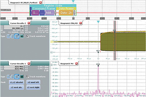
The RF output connects to channel one of the RTO and the time scale is set to 500 µsec so the complete settling time can be observed. The figure (top) shows the resulting measurement for a CW input signal at -10 dBm. The upper grid shows the decoded RFFE command where the trigger value of 0x02 is visible.
Note the trigger point denoted by the triangle at the top of the grid corresponds to the decoded value. The center grid shows the RF carrier and a math trace that computes the power envelope of the carrier. The trigger point also displays on this grid. There are two markers on the math trace showing the power before and after the PA switches on. The readouts to the left of the grid show the values at 130 nW and 516 µW respectively. The bottom grid shows the power spectrum of the carrier at a point 86.5 µsec from the trigger (receipt of the RFFE command). A marker at the peak indicates the power level of -2.87 dBm or 500 µW.
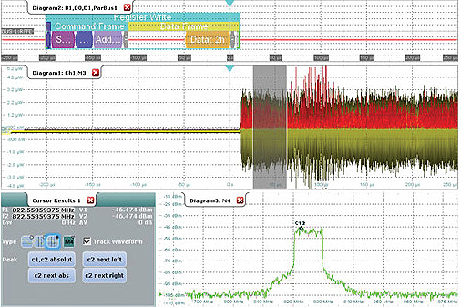
A similar configuration is measured in the figure below. In this case, the signal is an LTE carrier applied to the power amplifier. The spectrum in the lower grid is taken at a point 44 µsec from the trigger (also the decoded RFFE command).
References
Rohde & Schwarz,
www.rohde-schwarz.com
MIPI Alliance,
www.mipi.org

Leave a Reply
You must be logged in to post a comment.