Charge-coupled devices (CCDs) and complementary metal-oxide-semiconductor (CMOS) technology have been in fierce yet friendly competition. Fierce because valuable market share is contested, friendly because the rival digital camera technologies have much in common.
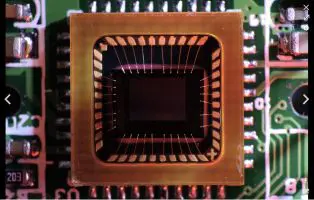
It is ironic that the more-costly CCD sensor is used in the most advanced astrophotography instruments and also in low-end point-and-shoot cameras, while CMOS sensors dominate the large mid-range market. CCD and CMOS sensors perform the same functions, converting light energy in the form of a focused beam of photons into an electrical output modulated by graphic information.
The CCD sensor has been likened to a bucket brigade. It is a current-driven device. It collects charge in its pixels (basically capacitive bins), then physically shifts the charge on the imager surface to the output for sampling. The output is an analog pulse where the charge is proportional to the light intensity.
Horizontal lines get shifted down the sensor into a horizontal shift register that send pixel contents to an A/D converter. CCDs generally provide better sensitivity and fidelity than CMOS imagers, but are slower because of the time needed to shift data down the display and through the shift register.
CCD sensors can experience performance issues because of their makeup. One is blooming, caused by charges from over-saturated pixels spreading to those nearby. This effect manifests itself as bright spots in the image that lack detail. A similar effect is blooming, also caused by saturated pixels. Here, charges spill over into the vertical shift register during the clocking-out process.
Full-well capacity in a CCD sensor refers to the fact that a CCD in light-gathering mode has a maximum number of electrons that can be stored under an individual pixel. It is undesirable to attempt to integrate a potential well beyond this point, at which saturation occurs. Then, additional electrons cannot be accommodated. This defines the upper limit in the dynamic range of a CCD sensor.
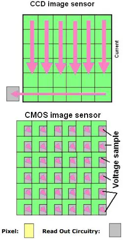
In contrast to CCDs, CMOS sensors are voltage-driven devices. Light striking the pixel creates a voltage proportional to intensity. The voltage is sampled at the pixel, digitized on the imager, and cleared for the next frame.
CMOS circuitry involves multiple layers of semiconductor material. The layer stack-up gives CMOS a lower charge conversion than CCDs, with an accompanying lower sensitivity (at least for older sensors). For the same reasons, CMOS imagers tend to have more image nonuniformities (fixed pattern noise) caused by unevenness between individual pixels and use of multiple A/D converters reading out the pixel columns. On the other hand, CMOS imagers have fewer problems with smearing and blooming. Moreover, their use of voltage sampling rather than buckets of charge make them more energy efficient than CCDs and with a faster readout.
One advantage of both CCD and CMOS digital imaging is that the camera can do on-board processing to correct some imaging problems. For example, it may be possible to adjust sensor output to handle high dynamic range images that would otherwise have bright parts of the image bleached out. It may also be possible to correct blemishes or for uneven illumination.
Image quality in CCDs and CMOS devices can be degraded by several effects. Temporal noise is the term given to anything besides light the causes a pixel value to change over time. Typical causes include quantization noise from the ADC process, shot or photon noise due to random fluctuations in the light (i.e. brighter/better light, less shot noise), and dark current noise caused by higher temperatures (doubles every 8°C, so cooler cameras = less dark noise). Spatial noise, also called fixed pattern noise, refers to constant nonuniformities in the image caused by bad sensor design, EMI, and similar effects.
Perhaps the most important measurement of image quality for digital sensors is signal-to-noise ratio. The SNR characterization curve is generally given as a graph of SNR vs. light density (typical units are photons/pixel or photons/unit sensor area) and is unique for a given imaging device. It can provide a way of comparing, for example, how different cameras behave at low light levels and high light levels.

For imaging applications in machine vision, there is an industry standard that dictates how to measure digital camera image quality. Called EMVA1288, it is managed by the European Machine Vision Association. It specifies testing conditions such as light levels, lenses, targets, and so forth, spells out how manufacturers should report data, allows apples-to-apples comparisons among different brands of sensors and camera equipment.
One important parameter that describes both CCD and CMOS sensors is quantum efficiency. Quantum efficiency of a photosensitive device is a measure of how many incident photons get converted into charge carriers. All photons do not have the same energy. The energy of a photon is inversely proportional to its wavelength. At various frequencies, the quantum efficiency differs. Both CCD and CMOS sensors may have a quantum efficiency of over 90%, in contrast to less than 10% quantum efficiency for photographic film. Quantum efficiency is one of the factors that determine overall digital camera SNR, along with other entities such as lenses and signal paths.


Excelent article