In a recent post, we reviewed the basics of Spice circuit simulators. Most circuit simulations involve transistors, either as discrete components or within an integrated circuit. So it is useful to understand a few basics about how Spice models transistors.
Transistors may have multiple states, typically saturation, cutoff, active and reverse. And transistors have an operating or quiescent point which is defined by dc biasing. As long as the operating point falls within a specific operating region the transistor will perform as defined in that specific state. But if the operating point crosses into another region, transistor operation changes.
Transistor models are developed to define the ranges for those regions and to select the best or optimal operating point or quiescent (Q) point around which operation can be maintained.
Typically, there are two classes of models for transistors. Large-signal models are used to determine the dc biasing of the transistor based on its configuration. For example, bipolar junction transistors (BJTs) have three common-mode configurations:
In common-emitters, dc current flows from collector to emitter and base to emitter. An ac signal is applied to the base and output is taken from the collector. In common-base circuits, dc current flows from collector to emitter and collector to base. An ac signal input is applied to the emitter and output taken from the collector. In common-collector circuits dc current flows from base to collector and collector to emitter. An ac signal input is applied to the base and output is taken from the emitter.
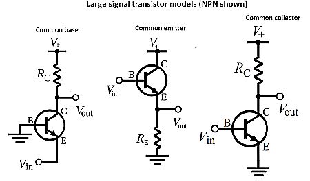 The common emitter is the most used of the three elementary configurations. An important characteristic is that it inverts the output with respect to the input, an effect that is eliminated if there are an even number of inverting stages.
Common-emitter circuits are afflicted with two common problems, both of which can be mitigated by proper circuit design. One difficulty is that in the common-emitter configuration, an amplifier may have a high gain, which tends to be unpredictable due to manufacturing variations, temperature and bias current. Automatic gain can take care of the variations, but along with them, the transistor in a common-emitter configuration can go into cutoff or oscillation, and the output can exhibit clipping.
Additional difficulties include low input dynamic range and high distortion. These problems, however, can be confronted by means of emitter degeneration, intentionally implemented by placing a resister between the emitter and the common signal source, which is often tied to ground or to one of the supply rails. (It is common practice to enhance stability by cutting back on the gain.)
A common-emitter amplifier often exhibits low bandwidth because of the Miller effect, which is applicable in inverting amplifiers. Any parasitic base-collector capacitance shows up as a higher capacitance between base and ground. The Miller effect can also be minimized by using emitter degeneration. Another stratagem is to reduce the output impedance of the signal source that is connected to the base.
Common emitters are frequently used as low-noise amplifiers in radio communications such as TV and Internet access satellite dishes, medical instrumentation and electronics test equipment, which frequently must operate close to the noise floor.
The common collector configuration is alternately termed an emitter follower. It is often used as a voltage buffer. Here the base is connected to the input and the emitter is connected to the output by being tied to ground or to one of the power-supply rails.
The emitter follower label comes from the fact that the circuit’s output is derived from the emitter resistor. Consequently, a frequent application for this device is as an impedance-matching circuit because its input impedance is higher than its output impedance. In conjunction with logic gates, it is used extensively in digital circuits.
Because the emitter follower voltage gain is roughly 0.6 V below the base, the common-collector transistor is considered an emitter follower. It is used for current gain and impedance matching rather than conventional voltage gain. Like the common emitter circuit, input impedance significantly exceeds output impedance.
The common-base configuration is frequently used as a current buffer or a voltage amplifier. The circuit input is fed to the emitter terminal and the collector is the output. Because the base connects to ground, it is common to input and output. The common-base configuration is less frequently used compared to the other two configurations because of its low input impedance and high output impedance, which are generally undesirable. It is, however, seen in high-frequency applications because the base separates the input and output, minimizing oscillations.
There is no phase inversion between the emitter and collector in the common base configuration, so input and output waveforms are in phase and the amplifier is non-inverting. One reason for the common-base amplifier’s limited applications is its low input impedance. The common-base output can be high, so it is referred to as a current buffer or current follower. Typically, the common-base amplifier has a current gain (alpha) close to one. However, the voltage gain can be between 100 and 2,000. It all depends upon the bias resistors.
 Small signal models are used once the large signal model has been determined. When a small signal is applied to the transistor, it moves the operating point away from the bias point along the I-V characteristic curve depending upon the amplitude of the applied signal. The circuit is usually set up so this deviation from the dc operating point make the transistor change its operating mode as, for example, going from the active region into cutoff.
Small signal models are usually two-port constructions and typically comprise either H-parameters, a hybrid-pi model or a T-model. H (or hybrid) parameters use Z (or impedance/open-circuit) parameters, Y (admittance/short-circuit) parameters, voltage ratio, and current ratios to represent the relationship between voltage and current in a two port network. H parameters help describe the input-output qualities of circuits where it is hard to measure Z or Y parameters (such as in a transistor). The Hybrid-pi (also called Giacoletto) model represents the BJT using the small-signal base-emitter voltage and collector-emitter voltage as independent variables and the small-signal base current and collector current as dependent variables. T or transmission models use relationships similar to those of hybrid-pi models but are typically arranged differently. Conversion of one type parameter to another is generally straightforward through use of matrix algebra manipulations.

The problem, though, is that parasitic elements may not be well defined, particularly for state-of-the-art transistors such as GaN or SiC power devices, and even more particularly when switching at high speeds. Parasitic inductances in power devices, for example, often are due largely to the wire bonds between the semiconductor itself and its packaging. Device makers continue to experiment with packaging options to reduce such parasitic effects, but because this effort is on going, parasitic models in Spice may not reflect the values seen in real devices. Consequently, an appreciable amount of experimentation may be necessary to accurately characterize the parasitics of modern semiconductors.



Leave a Reply
You must be logged in to post a comment.