Most bipolar junction transistors and field-effect transistors (FETs) have three terminals. In the BJT symbol, the base lead is perpendicular to and lands at the midpoint of a short line segment representing the semiconductor substrate. The emitter has an arrowhead embedded in the lead, so the remaining lead has to be the collector. If the arrow head points out, the device is an NPN transistor. Otherwise, it is the less-used PNP. Keep in mind the mnemonics “not pointing in” and “pointing in please”.
FET symbols can be distinguished by the fact that drain and source connections take off perpendicularly from the substrate, rather than at acute angles, diverging from one another. Another difference is that in the JFET the arrow head is in the gate lead, not in the drain, which corresponds to the BJT emitter. If this arrowhead points in, the MOSFET is a P-channel device. If it points out, the MOSFET is N-channel.
Schematic symbols and conventions for drawing schematic diagrams differ among nations and jurisdictions. In Europe, IEC 60617, which is the same as British Standard BS 3939, publishes relevant standards. In North America, ANSI Y32.2-1975, IEEE Standard 315-1975 and CSA Z99-1975 are substantially the same. As for logic functions, IEEE Standard 91/91a promulgates the graphic symbols, which are referenced in ANSI Y32.2/IEEE Standard 315. The standard in Australia is AS 1102.
One question that sometimes arises concerns how to discern when an NPN, PNP, or FET is the best choice for a given circuit application. A few general guidelines help in making the determination.
First consider the FET vs BJT question. BJTs, whether NPN or PNP, are current controlled whereas FETs are voltage controlled. What this generally means in practice is that the BJT switches on when its base-emitter diode conducts current. The diode turns on and conducts current when it becomes forward biased, and that happens at the same approximate 0.7-V level as for an ordinary discrete diode. Thus a bias of less than a volt between a BJT base and emitter is enough to turn on the transistor.
In contrast, the voltage-controlled FET typically can require on the order of 10 V at its gate to turn on. However, its gate input current is much less than the base current of a BJT. Thus FETs are generally the choice when its important to minimize input current/maximize input impedance. There are other differences between BJTs and FETs in terms of switching speed and gain, but input considerations tend to be the primary focus.
 That brings us to the NPN vs PNP decision. A current flowing into the base of the NPN turns on the transistor whereas a current flowing out of the base turns on the PNP. Thus the most common use for NPN devices is for switching the ground side of a circuit. PNP devices are used to switch from the positive side. For example, consider the simple case of a load and and a voltage source. An NPN device would go between the ground and the load with the other end of the load connected to the voltage source. A PNP would go between the voltage source and the load with the other end of the load connected to ground.
A more realistic example of the two uses is that involving a load driven by a logic device such as the digital output of an MCU. Suppose the load works from 12 V but the MCU logic is at 5 V on, 0 V off. The approach is to add an external 12-V supply and connect its -V output to GND of the MCU.
Here you can connect one side of the load to 12 V and use an NPN transistor to switch the other side to ground. A current through a resistor to the transistor base from the MCU I/O turns on the load. When there’s no current (digital output= 0 V) the load keeps floating and is turned off.
Conversely, you can connect one side of the load to ground and use a PNP transistor to switch the other side to 12 V. Current is delivered to the transistor base when the MCU I/O is 0 V, and the load turns on. However, to turn off the PNP transistor, its base must see 12 V because its emitter is at 12 V. So it may be necessary to add another transistor to convert the 5 V to 12 V to drive the PNP.
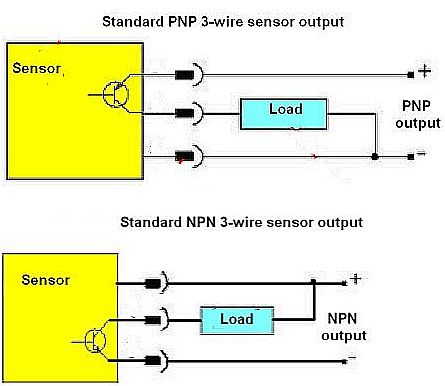
 NPN is a common configuration. Almost all open collector outputs are NPN outputs. The benefit of using a PNP is that the load only connects to the source when it is switched on. In contrast, one side of the load is always connected to the source when an NPN switches it on and off.
In the measurement field, the PNP/NPN issue most often arises in the use of industrial sensors. Industrial sensors can be found having either NPN or PNP outputs to control some load. Historically, Asian manufacturers standardized on NPN sensors (sourcing 24 Vdc inputs) while those in Europe generally use PNP (sinking 24 Vdc inputs).
Most U.S. plants standardize on PNP sensors as they are more widely used and easier to find than their NPN counterparts. And technicians often find PNP sensors easier to understand because the sensor produces a high-level voltage signal when the output is active.
 A point to note is that some manufacturers label inputs for the corresponding output device rather than for the actual function of the input itself.
An external pull-up resistor could be used to convert an NPN sensor to work with a sinking input. But this approach is a little tricky because it will invert the logic of the sensor. When the output of the NPN sensor is off, the sinking input will be pulled high. Alternatively, a pull-down resistor can be used to convert from PNP to NPN.


Leave a Reply
You must be logged in to post a comment.