By David Herres
Ordinary crystalline silicon semiconductors work according to the same physical principles as the old-world galena (PbS, lead sulfide) cat’s whisker radio-frequency detectors in early crystal sets. The defining element in a solid-state diode in the P-N junction. It is created when P-type and N-type slabs of crystalline silicon are joined. Wire leads are affixed to the two ends of the resulting usually tubular device so it can be configured along with other devices – resistors, capacitors, inductors, and so forth – to perform desired functions.

Diodes come in small sealed packages and cannot be opened up and repaired. Nevertheless, it is important to comprehend their internal mechanics to acquire insight into how the overall circuitry works. Moreover, comprehension of more complex semiconducting devices — including transistors, MOSFET’s, and ICs –builds on an understanding of how diodes work.
In an electrical circuit, the diode is analogous to a check valve in a water system. It conducts in one direction only. Because of this property, useful applications have emerged:
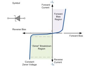
Blocking diodes prevent unwanted electrical backfeed, as in wind generators or photovoltaic solar arrays. Diodes can eliminate the portion of a waveform either above or below the zero level, thus converting ac to pulsating dc. Diodes can detect radio-frequency signals, suppressing the high-frequency component so that only the modulating envelope remains. Where reverse-bias breakdown voltage can be tolerated without destroying the device, as in a Zener diode, a diode can be placed in a shunt configuration so as to eliminate any voltage above a specific value, thereby providing regulation.

In an electrical circuit, the diode serves as a barrier to some portion of the current. But because this function is polarity dependent, the diode is considered an active as opposed to passive device.

Diode properties arise through the miracle of doping, where minute impurities are introduced into crystalline silicon, often by merely passing a gas over it. The prepared slabs become either N-type, with excess electrons, or P-type, with excess holes, which is just another way of saying the material has a deficiency of electrons.
Depending on how the diode is biased (which end is connected to which polarity), the electrons and holes are either repelled toward the P-N junction so the diode conducts, or attracted way from the P-N junction, so that the diode does not conduct.
If positive bias is applied to the anode, the diode will conduct.
That’s how this elegant little device works. It’s as simple as that.

Leave a Reply
You must be logged in to post a comment.