It is a fact, verified in theory and by experiment, that no material can conduct electric current with greater efficiency than an ideal conductor having zero resistance. How, then, can the term “negative resistance” have meaning in the real world?
First, it is possible to get negative resistance readings on a DVM. If this happens, they are generally anomalous and arise because the DVM settings are incorrect. Selecting the incorrect range on a DVM can result in the use of a test current that is too small. This will result in voltages too small for the DMM to measure. These small voltages will also be susceptible to other sources of errors that will offset the reading and possibly cause a negative measurement. The main sources of error include thermoelectric EMFs, offsets generated by rectification of RFI (radio frequency interference), and offsets in the voltmeter input circuit.
But it is, in fact, possible for a semiconductor device to exhibit a negative resistance. To see why we must first look at a standard resistor. In this modest component, there is a proportional relationship between the current passing through and the voltage applied to the (usually) two terminals. In contrast, a device that exhibits negative resistance is characterized by the applied voltage and measured current being inversely proportional, defying Ohm’s law.
You can connect the terminals of a standard probe across an energized negative resistance device and plug the probe output into the analog input of an oscilloscope. Simultaneously, you can connect a current probe that senses the magnetic field associated with either of the conductors to a different analog channel input. Displaying these signals together, the waveform amplitude relations are seen to vary for different portions of the phase. An understanding of this relationship is critical to seeing how conservation laws are not violated. That is because the negative differential resistance region does not occupy the entire phase.
If voltage is applied to a load with positive resistance, power transfers from the source to the load. Transfer of power in the case of positive resistance is a one-way path – from the power source to the load. Current flows first through a hot wire, through the load, and back along the return conductor to the power source.
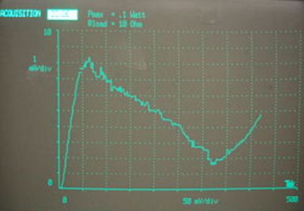
Negative resistance can be either static or differential. Static resistance is another term for the ordinary resistance that conforms to Ohm’s law. Differential resistance, also known as dynamic resistance, is the derivative of applied voltage with respect to measured current. Differential negative resistance happens when the electrical energy is in the form of alternating current.
Both dynamic and static resistance are measured in ohms, and of course, they conform to Ohm’s law. Unlike a simple resistor, a negative resistance component can amplify power, even if it has only two terminals. In a transformer, any rise in voltage is at the expense of current, so power cannot be amplified.
So the overriding question is, how can a two-terminal device with no power applied from an external source actually amplify power? The answer is that this can happen only throughout one portion of the ac cycle, so the law of energy conservation is not violated.
Negative resistance does not ordinarily arise in nature. That is because power into a load is equal to the current through the load times the voltage across it. With a negative resistance, still hypothetical at this point in the discussion, instead of dissipating electrical energy in the form of heat, it would actually generate electrical energy and feel cool to the touch. The explanation for this non-intuitive state of affairs is that the voltage and current would have opposite signs. (A negative value times a positive value is a negative value.)
When voltage is applied to a passive device that exhibits negative resistance in some part of its response curve, the device outputs power, but that happens only during the period when voltage as a function of current is negative. The device outputs power when it is operating in the second and fourth quadrants of its response curve, but unfortunately for the perpetual motion community, this is only power that is stored when the device operates in the first and third quadrants.
A statement that defines one aspect of negative resistance is that those few devices that exhibit it experience a drop in current as more voltage is applied across their terminals. This behavior is opposite to that of a standard positive resistance, where voltage and current vary directly. Accordingly, a two-terminal device can be made to amplify an ac signal applied at the terminals. Examples are tunnel diodes and Gunn diodes.
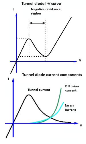
Tunnel diodes, first manufactured by Sony in 1957, have negative differential resistance within a prescribed operating range. They employ a quantum mechanical effect known as quantum tunneling, which lets them operate as negative resistances at high frequencies, well into the microwave region.
Like all diodes, tunnel diodes have a PN region. But it is heavily doped and unusually narrow. This creates a band gap in which conduction band electron states on the N side align with valence band hole states on the P side.
The prevalent semiconducting material used in tunnel diodes is germanium. Gallium arsenide and silicon are alternatives. Because tunnel diodes have negative differential resistance in a portion of their operating range, they are used in frequency converters and detectors. The explanation for negative resistance in a tunnel diode is that when the diode is forward biased, a rising applied voltage lets electrons tunnel through the P-N junction because it is quite narrow, typically 10 nm.
When forward bias voltage is low, the conduction states on either side of the junction barrier are closely aligned. But as this voltage rises, the conduction states on either side become misaligned. For this reason, the current flow drops as the voltage rises, giving the device a negative resistance differential. As still higher voltage is applied, operation shifts from tunneling to the normal diode mode. What is unique in a tunneling diode is its reverse-bias operation, where the device is a fast rectifier with no offset voltage and highly linear behavior.
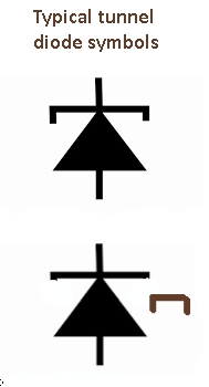 The tunneling diode, when forward biased, exhibits quantum mechanical tunneling. Boosting forward voltage causes forward current to drop, and this exemplifies negative resistance. These qualities make the device suitable for low-noise microwave applications. In the past they were also used in oscilloscope triggering circuits. In recent years, the FET and other non-diode, three-terminal devices have replaced tunneling diodes, notably in local oscillators for superheterodyne receivers.
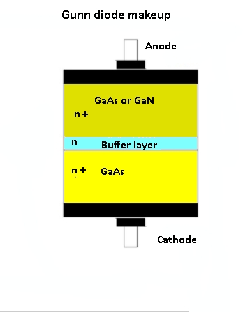 The Gunn diode is another component that exploits negative resistance. It is also known as a transferred electron device, another high-frequency component, currently found in law-enforcement speed detection equipment, commercial door openers and microwave relay links. Most diodes have P- and N-doped layers, but Gunn diodes employ N-doped regions exclusively. Unlike other diodes, Gunn devices do not conduct directionally, which means that they cannot function as rectifiers. There are three active layers, two N-doped with a thin N-doped region situated in the middle. In normal operation this middle layer exhibits the greatest voltage drop. As higher voltage is applied, the Gunn diode becomes a negative-resistance device. Accordingly, the Gunn diode in this mode operates as an RF amplifier. When dc voltage is applied, the diode goes into oscillation, making it useful in other high-frequency applications.
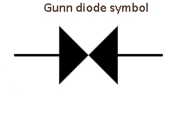 Gunn diodes are used at the highest frequencies. Among devices that exploit negative resistance, they are noted for high output power. Gunn diodes have applications that include anti-lock brakes, radar for aircraft collision avoidance, amateur radio transmission, security alarms and radio astronomy.
Electric discharge lighting such as neon and fluorescent fixtures are common devices exhibiting negative resistance. A heavy voltage drop due to utility power applied across the terminals could cause a fluorescent bulb to rupture, so for this reason, a ballast, mounted inside or outside the enclosure serves to mitigate the effects of negative resistance.
Power sources for negative resistance components include batteries, solar arrays, fuel cells, generators and transistors. Negative resistance applications, besides those mentioned above, include active resistors and, where positive feedback is installed, feedback oscillators, negative impedance converters and active filters.
The behavior of negative resistance circuitry is complex, sometimes difficult to understand, because of the way it appears to operate contrary to common sense. Being nonlinear, negative resistance actually varies with the applied voltage, and that is sometimes hard to deal with. But as functioning components, negative resistance devices conduct electricity and permit the circuits in which they appear to do work and play useful roles in contemporary circuit designs.

Not even wrong.
The statement that “energy is conserved over the cycle” is an example. Resistance is negative because the semiconductor device is active and capable of drawing energy from the background power source for generating energy instead of dissipating energy.