Most engineers are familiar with charge-coupled devices (CCDs) employed as image sensors. Pixels in a CCD sensor consist of P-doped metal-oxide semiconductor capacitors arranged in columns and rows to form an array. Light striking each pixel is converted to an electrical charge that varies according to the light intensity at that pixel. The CCD transfers the charge from one row of pixels to the next bucket-brigade style until it reaches the edge of the chip where it is converted to a digital pulse even as another row moves across the array.
In recent years CMOS image sensors have improved to the point where they compete with CCD devices. CMOS sensors are faster than their CCD counterparts, allowing higher video frame rates. CMOS imagers also provide higher dynamic range and require less power to operate. But CCDs are more sensitive to infrared light than CMOS sensors. This is an advantage in astrophotography. (In fact, there are YouTube videos explaining how to turn inexpensive CCD cameras into IR cameras simply by removing the IR filter that sits in front of the CCD sensor in the camera.)
 Nevertheless, when it comes to thermal imaging, CMOS sensors are not the main competitor to CCD sensors. Rather, the other go-to image sensor technology is the microbolometer. Here each pixel in the image-sensing array is a microbolometer–basically a temperature-sensitive resistor. Electronics in the sensor substrate convert the resistance change to a voltage. These sensors do not require active cooling, unlike many infrared imagers, greatly simplifying the imaging process.
To explain where CCDs and microbolometers excel, it is useful to back up a bit and briefly review the way bodies emit heat. Wien’s law expressed mathematically as λmax = C/T explains the relationship between an object’s temperature and the peak wavelength it emits. Here C is a constant, 2,897 μm, and T is the object’s temperature in degrees Kelvin. Thus the higher the object temperature, the shorter the peak wavelength. For example, a normal human who isn’t running a fever is about 310.15°K and emits a peak wavelength 3.94 μm. The sun averages 5,778°K and has a peak wavelength of about 0.5 μm. (Note that light from stars are subject to significant Doppler effects which affect their perceived wavelength on earth.)
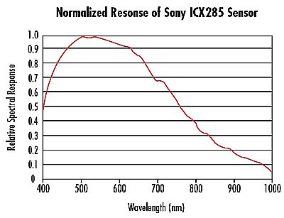
Now consider that CCD and CMOS sensors are sensitive to wavelengths from approximately 0.350 to 1.05 μm, although the range is usually given from 0.4 to 1.0 μm. Most CCD cameras provide an infrared cut-off filter for imaging specifically in the visible spectrum. (Hence the YouTube videos.) In contrast, microbolometers excel at detecting infrared radiation with wavelengths between 7.5–14 μm, the range spanning emissions from living creatures.

Dark current. of course, is current flowing even if no light hits the sensor. It is caused by thermal excitation of electrons in the InGaAs material. Dark current rises with sensor temperature. As a rule of thumb, it doubles about every 9°C.
Sensor temperature also greatly influences the spectral sensitivity of SWIR cameras. When sensor temperature drops from 25°C to -15°C the spectral sensitivity shifts about 25 nm toward lower wavelengths. The shift can be important for applications operating at the extreme ends of the sensitivity curve. Additionally, dark current impacts image quality (black level and noise). Thus it’s common to see thermal cameras operating in this range incorporate thermoelectric coolers (i.e. Peltier modules) sandwiched to the imaging IC.


Leave a Reply
You must be logged in to post a comment.