• Skip to primary navigation
  • Skip to main content
  • Skip to primary sidebar
  • Skip to footer

Test & Measurement Tips

Oscilloscopes, electronics engineering industry news, how-to EE articles and electronics resources

  • Oscilloscopes
    • Analog Oscilloscope
    • Digital Oscilloscope
    • Handheld Oscilloscope
    • Mixed-signal Oscilloscope
    • PC-based Oscilloscopes – PCO
  • Design
  • Calibration
  • Meters & Testers
  • Test Equipment
  • Suppliers
  • Video
  • EE Learning Center
    • Design Guides
      • WiFi & the IOT Design Guide
      • Microcontrollers Design Guide
      • State of the Art Inductors Design Guide
  • FAQs
You are here: Home / oscilloscope measurements / The ups and downs of bad DACs

The ups and downs of bad DACs

May 27, 2022 By David Herres Leave a Comment

A digital-to-analog converter (DAC) is more prone than an analog/digital converter to signal degradation. DACs are complex devices requiring precisely matched components. For this reason, with notable exceptions, DACs are implemented as mixed-signal ICs based on MOSFET technology. Discrete component DACs are found in radar systems and high-speed test equipment including digital sampling oscilloscopes.

Digital sampling may introduce quantization error that appears as noise in the reconstructed signal. It is here that we find DAC more problematic than the smooth-flowing ADC. DACs must be evaluated based on numerous criteria that generally include resolution, speed, dynamic range, SFDR (spurious-free dynamic range), ENOB (effective number of bits), and SNR (signal to noise ratio). One quality unique to DACs is the undesirable image signals appearing within each Nyquist zone of the output. Other important characteristics include settling time and glitch-impulse area. Settling time refers to the time it takes from the input code application until the output arrives at, and remains within, a specified error band around the final output voltage

glitches
Glitch impulse qualities as illustrated by Analog Devices.

ENOB is significant in establishing the real-world dynamic range of an DAC and arises from noise within the signal and from the DAC circuity, effectively reducing the DAC’s true resolution, SNR, and dynamic range. Other factors that can cause a real device to deviate from the transfer function of an ideal DAC include offset errors and gain errors (due to temperature fluctuations), differential linearity error, and total unadjusted error (TUE), among others. Clock jitter and thermal noise can trigger further errors deviating from ideal DAC performance.

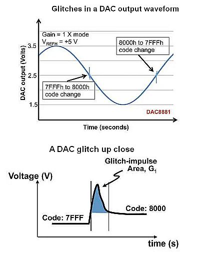
Glitch-impulse area is another important DAC quality. The glitch impulse is defined as the voltage transient appearing at the DAC output during a “major-carry transition.” It means during a single code transition, a MSB changes from low-to-high while LSBs are changing from high-to-low, or vice versa (i.e., a code transition from 0111 to 1000). The glitch impulse energy is equivalent to the area under the curve on a voltage-time graph. This glitch impulse arises because real circuits don’t move from one conversion value to the next monotonically, thus inducing glitch energy into the output and in turn degrading the DAC SFDR.

DAC images
DAC output can be represented as a series of rectangular pulses having a width equal to the reciprocal of the clock rate. Images of the fundamental signal arise as a result of the sampling function. Real DAC circuits often attenuate them by including an inverse sin(x)x filter.

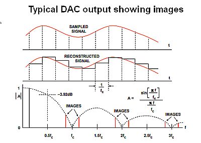
There are two approaches to minimizing glitch energy: Place either an RC filter or a S/H capacitor and amplifier after the DAC. The first approach lengthens settling time, though, while the second approach adds components and PCB space. To eliminate images within Nyquist zones, an anti-imaging filter is generally placed after the DAC.

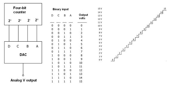
It is interesting to review what the output of a DAC looks like both when it is working and when there are problems. Suppose we have a four-bit DAC that receives inputs from a four-bit counter that produces a sequence of binary numbers from 0000 to 1111 and then recycles to 0000. Further suppose the DAC produces 1 V for each digit so 1111 (15 decimal) results in a 15-V output. If the DAC works properly, the output display on a scope will be the well-known staircase waveform.

staircase
The logic table and voltage output when everything is working in a DAC.
bad input
What you’ll see on a scope when a DAC input is shorted.

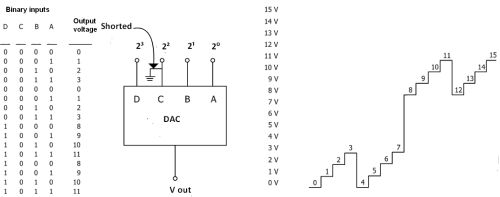
Now suppose one of the DAC inputs is shorted, in this case the input corresponding to the 22 binary value. The most straightforward way of figuring out which input is problematic is to compare the table of analog output voltages vs binary inputs to what’s seen on the scope display. In this case, the analog output voltage is zero at the 22 binary value. This is what’s known as a clue.

You may also like:

  • music on scopes
    Making pictures from sound on an oscilloscope
  • Havana syndrome
    Microwaves and the Havana Syndrome

  • Will your Good Samaritanism in the pandemic buy you a…
  • rental instruments
    The modern economics of renting test instruments
  • no you can't detect ghosts with a gauss meter
    No, you can’t detect ghosts with a gauss meter

Filed Under: FAQ, Featured, oscilloscope measurements Tagged With: analogdevices, FAQ, texasinstruments

Reader Interactions

Leave a Reply Cancel reply

You must be logged in to post a comment.

Primary Sidebar

Current Digital Issue

A frequency you can count on There are few constants in life, but what few there are might include death, taxes, and a U.S. grid frequency that doesn’t vary by more than ±0.5 Hz. However, the certainty of the grid frequency is coming into question, thanks to the rising percentage of renewable energy sources that…

Digital Edition Back Issues

Oscilloscopes Finder

Search Millions of Parts from Thousands of Suppliers.

Search Now!
design fast globle

Subscribe to our Newsletter

Subscribe to test and measurement industry news, new oscilloscope product innovations and more.

Subscribe Today

EE TRAINING CENTER CLASSROOMS

EE Classrooms

RSS Current EDABoard.com discussions

  • Measure AC current accurateley (100mA to 10A)
  • Mosfet SSR triac output shunt circuit design
  • Tessent MBIST for memories with dedicated test clock
  • Very low voltage/power Schmitt trigger?
  • Natural Convection Heatsink for 80W power dissipation?

RSS Current Electro-Tech-Online.com Discussions

  • Best way to reduce voltage in higher wattage system?
  • surge arresters
  • Someone please explain how this BMS board is supposed to work?
  • Need a ducted soldering fan for solder smoke extraction
  • DIY bluetooth speaker

Footer

EE World Online Network

  • DesignFast
  • EE World Online
  • EDABoard
  • Electro-Tech Online
  • Analog IC Tips
  • Microcontroller Tips
  • Power Electronic Tips
  • Sensor Tips
  • Connector Tips
  • Wire and Cable Tips
  • 5G Technology World

Test & Measurement Tips

  • Subscribe to our newsletter
  • Advertise with us
  • Contact us
  • About us
Follow us on TwitterAdd us on FacebookFollow us on YouTube Follow us on Instagram

Copyright © 2022 · WTWH Media LLC and its licensors. All rights reserved.
The material on this site may not be reproduced, distributed, transmitted, cached or otherwise used, except with the prior written permission of WTWH Media.

Privacy Policy